PCB tool innovation from the middle out
Mid-market users are driving richer features and cost competition into PCB design software like never before, largely thanks to the Internet of Things.
As the focal point for eastern electronics moved from May’s inaugural CES Asia in Shanghai to June’s more established Computex in Taipei, an interesting trend in PCB design became clearer. The middle-ground is shifting, and indeed moving rapidly upward in terms of complexity.
Once upon a time, PCB design was crudely broken down into three groups: hobbyists, commodity board stuffers, and enterprise users. However, these definitions are not proving too helpful today (if they ever really were), even where the end-focus a lower-tier company might still be a ‘me too’ product.
The boards for low-cost smartphones helped accelerate the shift, but Asian entrepreneurs are now also looking to achieve cost-effective designs for equivalents to the likes of Google Glass and the Oculus Rift 3D headset. Those ain’t simple, particularly if you don’t want to find yourself on the wrong side of a nasty lawsuit.
Perhaps more importantly though, Asian governments are pushing local design companies to focus on the Internet of Things, particularly China. Its cumulative investment in IoT technology and machine-to-machine infrastructure will reach a staggering $600B by 2020, according to the GSM Association.
IoT design requires both innovation (the IoT truly is a case of ‘What China does today…’) and then complex implementation often within the smallest possible form factor.
But there’s a catch when it comes to the implications for PCB design and the tools serving the market: much of China’s IoT activity is being funneled through start-ups. These are fledgling systems design companies that it needs to achieve its five-year economic plan goal of, ‘From made in China to created in China.’ But they typically do not yet have the $50,000/seat resources to buy full enterprise level PCB design tools and support.
So, something has had to give. The major PCB design tool vendors are drawing more sophisticated functionality into their mid-market and entry-level suites.
PCB design’s new middle ground
Cadence Design Systems has been adding assiduously to its now 30 year-old warhorse OrCAD. Altium recently opened up its basic CircuitMaker tool to a ‘community-driven’ beta test, aimed at getting users to help determine the breadth of functionality it should offer.
However, the largest PCB design tools vendor, Mentor Graphics, has now moved to most explicitly reflect the shifting trend not just in features but also in how it markets and tiers its software.
Mentor spent much of 2014 and 2015 rolling out a wide-ranging update to its flagship, high-end PCB design suite, Xpedition Enterprise. But in April, it announced a further three-way split across its mid-tier ‘out of the box’ sister, PADS.
This is now available in three flavors: PADS Standard, PADS Standard Plus and PADS Professional. Figure 1 shows how new and existing features are gradually added as a user buys in – and, Mentor then hopes, through – to the different levels.
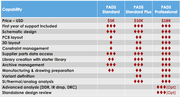
The three new PADS PCB design options (Mentor Graphics)
“The industry ecosystem has become a lot more complex than it was a few years ago, and particularly at this level that we think of as the independent project-based engineer,” says Paul Musto, Mentor’s product line manager for PADS.
“To take one example, about 10-15 years ago, you had a lot of vertically integrated companies and they would do much of the design themselves. Also, they had a lot of experts within those companies – experts in routing, experts in power and signal integrity, experts in DFM and so on. We still serve that model and those specialist use-cases with Xpedition. A lot of Xpedition business is more à la carte.
“But now we see a lot of those companies outsourcing parts of a design, even complete designs. And they’ll often do that to a smaller operation where rather than specialists, you have one group of engineers working across multiple areas. The single-view has always been part of PADS. But as the business models have changed, the number of areas those project-based engineers has seriously grown. So it’s a big evolution.
“Then you do have the emergence of the Internet of Things. Again, a lot of these companies are still pretty small, and a single engineer has to work in many fields. They’re also getting into much more complex technologies.”
That is the context for not only splitting PADS but also, as Mentor hopes some users progress up its different levels, making a later step-up to Xpedition possible.
“We had a market that used to be separated between high-end enterprise, and lower-end simpler technology. The lines now though are a lot more blurred,” adds Musto.
PCB design tool innovation
Another intriguing aspect of what the PCB design tool vendors are looking to achieve shows innovation in their products now being driven both from the top-down and also from the middle-out. This is not solely being driven by the IoT.
For its community beta, Altium has explicitly reached out to the maker community. “We’re incredibly excited to see how the CircuitMaker community will grow and evolve during this open beta program,” said Ben Jordan, Altium Product Manager at the scheme’s launch. “The electronics maker community has always been characterized by a very organic and collaborative growth process.”
Meanwhile David Wiens, business development manager at Mentor, also points to an increase in tool use-models where a new product may start its life in a PADS environment before later being moved to the higher-end Xpedition for full implementation.
“Within a big company, you can have a prototyping or a proof-of-concept team that looks like this independent project-based model. It’s just one engineer or a couple of engineers looking to get a project started and they too need a single, unified environment,” says Wiens.
“They could be sitting in a large enterprise but more independent of the larger organization. You could even call them renegades, but they’ve got a job to do.”
This all diverges from EDA’s traditional model – and one that still seems prevalent at the silicon-design level – were innovation is overwhelmingly driven by Tier One customers and the demands raised by incoming process nodes or the need for further reductions in power.
Although yes, Mentor did update Xpedition first.
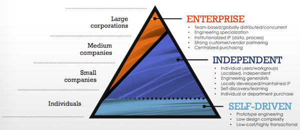
Mentor’s view of a shifting, overlapping PCB design sector (Mentor Graphics)
PCB design cost pressures
One other area where PCB and silicon tools have long diverged is cost. PCB is a far more price-sensitive market.
With Mentor going public on the price range for its three flavors of PADS, it is worth noting that these pretty much remain within the existing ballpark for the market.
Before, a fully featured PADS suite including the main options would have cost around $13,000/seat. Altium Designer, meanwhile, comes in at around $10,000. With the new PADS price structure from $5,000 to $18,000, Mentor is not trying to push the envelope that far, though there is an aggressive price-cut at the entry-level.
“We think there’s a very big volume of customers who will look at PADS Standard at $5,000 and see a good deal,” says Jamie Metcalfe, market development manager at Mentor. “The numbers for PADS Professional will be smaller, but then the return on each sale will be greater.”
The key to maintaining the current level of innovation in features may be what opportunites this price model ultimately delivers for the up-sell, both within the PADS universe and beyond.
PCB design tools have suddenly got a lot more interesting and, yes, we probably do have the Internet of Things – and Asia’s ambitions for it – to thank for that.
The challenge ahead may lie in harnessing the dynamics of the ongoing move-down in design complexity to sales numbers that will encourage the vendors to keep pushing their latest technologies into the mid-market more quickly than in the past.
The good news is that there are all those start-ups who need some way to do the job and can provide some initial volume on mid-range tool sales. Returning to China’s explosive progress, Wan Gang, the country’s science and technology minister, recently claimed that the Zhongguancun electronics incubation district in Beijing alone generated an average of 49 new companies every day in 2014.
Not all of those will want Designer, OrCAD or PADS, but a fair few will. If, in time, even only a small number of those grow into enterprise-level users….