Multiple cross clock domain verification
Today’s system-on-chip designs often need to encompass multiple asynchronous clocks. This raises the problem of verification for the resultant clock domain crossings.
It is becoming apparent that functional simulation alone is not up to the task. Instead, engineers need to consider hybrid methodologies, combining structural and functional verification approaches.
The use of assertions is also proving increasingly important to CDC verification, and the author provides examples of code he built to address the techniques and features demanded by increasingly complex designs.
The design of multi-million-gate system-on-chips (SoCs) is made still more complex where engineers must account for the presence of multiple asynchronous clocks. The problem is not uncommon—for example, different external interface standards such as PCI Express (PCIe) and Internal Bus (IB) use different clock frequencies. Another factor can be the additional presence of a single fast clock that is effectively distributed over the entire chip.
The verification of such designs has become especially tedious, time-consuming and therefore costly. Moreover, traditional functional simulation is proving inadequate for the verification of clock domain crossings (CDCs). Instead, this article describes a methodology for verifying the synchronization of different asynchronous clock domains that uses both structural and functional verification techniques. It also outlines the use of an assertion-based verification strategy that can be added to a simulation-based flow to improve design quality.
SoCs with interfaces like PCIe and IB have two different operating frequencies and require synchronization during data transfer. Failing to synchronize data and control transfers between asynchronous clock interfaces leads to timing violations (e.g., setup and hold time) that cause signals to enter a metastable state. These metastable timing errors are difficult to detect as they are randomly generated. To detect them, you need the right combination of clock edges and data.
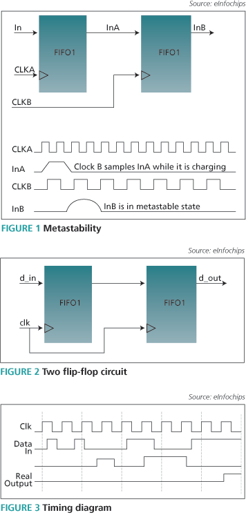
Metastability
The proper operation of a clocked flip-flop depends on the input signal being stable for a certain period of time before and after the clock edge. If the requirements for setup and hold time are met then a valid output will appear at the output of the flip-flop after a maximum delay. But if the requirements are not met, the signal will take much longer to reach a valid output level. We refer to the result as either an ‘unstable state’ or ‘metastability’ (Figure 1).
Metastability is avoided by adding various features to a design. Two of the most common such features are:
- two flip-flop circuits (this technique requires a stable design since incorrect design will lead to synchronization failure); and/or
- FIFO buffers (handshaking mechanisms).
Structural clock domain verification
Structure analysis checks the connectivity and combinational logic of a design. It should be performed on both the RTL code and the post-synthesis gate-level netlist. It can be performed by using automated CDC tools, scripts-based verification and code review, and identifies the following issues:
- unresolved clocks;
- combinational logic failures ( jitter and glitches); and
- insufficient synchronization of signals where synchronizers are based on flip-flops.
Functional clock domain verification
Structural analysis will find annoying errors. However, it alone will not verify whether synchronizers have been used correctly in the design. Here, we pull upon functional analysis techniques as they can identify the following types of issue:
- data stability between two different clock speeds (fast and slow);
- FIFO read and write when both pointers operate on different clock frequencies; and
- data stability with a handshake-based synchronizer.
To identify synchronizers, functional clock domain verification uses the same algorithm as structural verification. However, under functional verification, assertions can be implemented for each type of synchronizer and as checks on all possible input conditions. Clock domain analysis with assertions can also be performed at different levels (e.g., block-level, full chip-level and gate-level) and helps to detect real timing violations in the gate-level simulation.
Let’s now explore in more detail two of the design features used to overcome metastability.
1. Two flip-flop circuit
A two flip-flop circuit is used to add delay for synchronization on a signal path. For the example shown in Figure 2, input data values must be stable for three destination clock edges. There are three cases where the input will not be transferred to the synchronizer output—where it is sampled by only one clock edge, sampled by two clock edges or not sampled by clocks at all.
The advantage of a two flip-flop synchronizer is that it filters the metastability state, and this process is shown in Figure 3. The first ‘d_in’ pulse is never sampled by the clock and will not be transferred to ‘d_out’. But if the rising edge of this pulse violates the previous hold time or the falling edge violates the current set up time, this value may propagate to the real circuit.
The second ‘d_in’ pulse is sampled by the clock, but if this signal changes just before the clock edge because of a setup time violation, the simulation will transfer the new value. In this case, the real circuit will become metastable and will transfer the original low value.
The third ‘d_in’ pulse is sampled by two consecutive clock edges and will be filtered by the synchronizer. Since the rising edge of ‘d_in’ violates the setup time for the first clock edge and the falling edge violates the hold time for the next clock edge, simulation will propagate two clocks.
Here are the assertions and related descriptions required during this step.
To check stability of the data:
property stability;@(posedge clk)!$stable(d_in) |=> $stable(d_in) [*2];endproperty : stabilityTo check for a glitch:property no_glitch;logic data;@(d_in)(1, data = !d_in) |=>@(posedge clk)(d_in == data);endproperty : no_glitchassert property(stability);assert property(no_glitch);
The ‘stability’ assertion checks the stability of ‘d_in’ for two clocks. The ‘no_glitch’ assertion checks for a glitch on ‘d_in’.
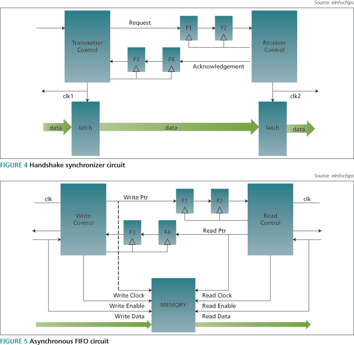
2. FIFO buffer circuits
2.1. Handshake synchronizer
Different types of handshake synchronizers are used to avoid CDC. In the type shown in Figure 4, the transmitter sends a request that is synchronized by two flip-flops. Here, the number of flip-flops is not fixed as it depends on the frequency of the clock. Once the receiver receives a request, it latches the data and sends an acknowledgement back to the transmitter. In this case, the data must be valid when the request is asserted.
If the request is not synchronized properly because of flip-flop error, it can be caught during structural verification. That step identifies errors that arise when incorrect data is latched through glitches generated by combinational logic driving a flop-based synchronizer.
Insufficient synchronization is also a structural error. High-speed clocks require a greater number of flip-flops and any shortfall can be detected by structural verification.
For verification of the handshake synchronizer circuit, the following conditions can be asserted:
- Every request gets acknowledged.
- No acknowledgement without a request.
- Data stability.
Here are the assertions and related descriptions required for this stage.
Every request gets acknowledgedsequence req_transfer;@(posedge clk)req ##1 !req [*1:max] ##0 ack;endsequence : req_transferproperty req_gets_ack;@(posedge clk)req |-> req_transfer;endproperty : req_gets_ackNo acknowledgement without requestproperty ack_had_req;@(posedge clk)ack |-> req_transfer ended;endproperty : ack_had_reqData stabilityproperty data_stablility;@(posedge clk)req |=> data [*1:max] ##0 ack;endproperty : data_stablilityassert property(req_gets_ack);assert property(ack_had_req);assert property(data_stablility);
The ‘req_transfer’ assertion checks whether every request gets acknowledged. The ‘ack_had_req’ assertion checks whether every acknowledgement has a request. The ‘data_stability’ assertion checks if the data is stable for the period of the request, including an acknowledgement.
2.2 Asynchronous FIFO circuit
A dual clock asynchronous FIFO circuit is used for CDC synchronization when high latency in the handshake protocol cannot be tolerated. The circuit changes according to the requirements of the SoC but its basic operation is constant (Figure 5). Data is written into the FIFO from the source code and read from the FIFO in the destination clock domain.
Read and write pointers are passed into different clock domains to generate full and empty status flags. Data write and read is kept in synchronization by write and read pointer positions.
The following conditions can be asserted for verification of dual FIFO asynchronous circuits:
- Data integrity.
- Do not write when the FIFO is full.
- Do not read when the FIFO is empty.
Here are the assertions and related descriptions for this step.
Don’t write when FIFO is full/Don’t read when FIFO is emptyproperty full_empty_access(clk, inc, empty_full_flag);@(posedge clk)inc |-> !empty_full_flagendproprty : full_empty_accessData integrityint write_cnt, read_cnt;always@(posedge write_clk or negedge write_rst_n)if (!write_rst_n) write_cnt = 0;else if (winc) write_cnt = write_cnt+1;always@(posedge read_clk or negedge read_rst_n)if (!read_rst_n) read_cnt = 0;else if (rinc) read_cnt = write_cnt+1;property data_integrityint cnt; logic [DSIZE-1:0] data;disable iff (!write_rst_n || !read_rst_n)@(posedge write_clk)(winc, cnt = write_cnt, data = wdata) |=>@(posedge read_clk)first_match(##[0:$] (rinc && (read_cnt == cnt)))##0 (rdata == data);endproperty : data_integrityassert property(full_empty_access(write_clk,winc,wfull));assert property(full_empty_access(read_clk,rinc,rempty));assert property (data_integrity);
The ‘full_empty_access’ assertion ensures that there should not be data access when FIFO is empty and FIFO is full. The ‘data_integrity’ assertion starts a new thread with an initial count value whenever data is written into the FIFO, and checks the read data value against a local data variable whenever a corresponding read operation occurs.
CDC jitter emulation
One problem that can arise because of synchronization is CDC jitter. Even though all signals may be synchronized properly for the destination clock domain, the actual arrival time can become uncertain if the signal goes metastable in the first synchronization flip-flop. This CDC jitter can lead to functional failures in the destination logic.
Normally, this jitter would not show up on a simulation. Both formal and dynamic verification methodologies can be used to determine if the design still works with CDC jitter. Formal verification can prove that design properties are never violated for all possible jitter conditions whereas simulation can only demonstrate that no assertion checks are violated for a particular jitter combination. Actual violations can also be difficult to debug in simulation. CDC jitter emulation provides an improvement in overall verification quality.
Gray encoding
In addition to handshake-based and FIFO-based synchronizers, another method of synchronizing data is first to gray encode it and then use multi-flop synchronizers to transfer it across domains.
For multibit signals, a gray code ensures that only a single bit changes when a group of signals counts. This makes it possible to detect whether all the bits have been captured by the receiving clock together or if they have been skewed across multiple clock cycles due to metastability.
Another example is in an asynchronous FIFO where the read and write pointers cross the write and read clock domains respectively. These pointers are control signals that are flop-synchronized. The signal is gray-encoded prior to the crossover.
This can be verified using assertions. The assertion is simply exclusive-or of the data and the previous value of the data with the condition that it must have at most one active bit (i.e., it should be ‘one hot’).
The relevant assertions statement is shown here:
property check_graycoded =always ((gc == 8’h0) || (((gc ^ prev(gc)) &((gc ^ prev(gc)) – 8’h1)) == 8’h0));assert check_graycoded;
All the assertion statements in the examples above verify that the receiver gets the expected data. Since the latency between sending and receiving data is not known, verifying the sequence will ensure that no data gets dropped.
The actual value in the data sequence should not make a difference to the verification; an assertion could be written using a more random sequence or specific data values.
Formal verification can use this assertion to verify that the control logic of the assertion does not allow any loss of data and will generate counter example traces if any failures are found.
Conclusion
Multiple cross clock domain verification is best performed using both structural and functional verification techniques. The verification process may start with structural verification to remove errors related to insufficient synchronization, combinational logic driving synchronizers or missing synchronizers. After structural verification, functional verification may be used to implement additional assertions and check the usage of the synchronizers.
eInfochips, Inc.
1230 Midas Way
Suite# 200
Sunnyvale
CA 94085, USA
T: +1 408 496 1882
W: www.einfochips.com