MEDEA: a hybrid shared-memory/message-passing multiprocessor NoC-based architecture
This paper describes Medea, a NoC-based framework that uses a hybrid shared-memory/message-passing approach. It has been modeled in a fast, cycle-accurate SystemC implementation enabling rapid system exploration while varying several parameters such as the number and type of cores, cache size and policy, and specific NoC features. Also, each SystemC block has its RTL counterpart for physical implementation on FPGAs and ASICs.
This paper is an edited version from that presented at DATE 2010 earlier this year. A full version is available in the conference proceedings. For more information, go to www.date-conference.com. Since the paper was originally written, Sergio Tota has left the Politecnico di Torino and now works at Imagina- tion Technologies.
Introduction
The increasing number of cores that can be integrated in a die is stimulating a revolution in the microprocessor industry. General purpose architectures and domain-specific multicore architectures (e.g., graphics processing units (GPUs)) are switching from the use of a few complex out-of-order processors to many smaller and simpler in-order architectures.
The communication infrastructure plays a key role here. Current implementations use bus or ring network solutions, but these will not scale sufficiently to handle next-generation multicore architectures. The use of packet-switched on-chip networks (more simply network-on-chips or NoCs) is now widely accepted. These NoCs provide efficient and scalable communications subsystems by using switches placed according to a regular topology.
The scalability of the programming model is another issue. The classic shared-memory paradigm faces a performance roadblock attributable to the standard memory-hierarchy. Message passing has been used to achieve efficient, parallel communication in cluster-based systems. That technique now seems open to being extended into the new processing environment as it looks like an effective cluster-on-chip. In particular, the message-passing paradigm allows synchronization as well as data-exchange among different cores to be done in parallel because it uses a distributed low-latency on-chip network that needs no need access to a shared memory resource even if a shared memory programming model is fully supported.
In this context, we propose the Medea framework, a configurable hybrid shared-memory/message-passing architecture. Instructions for fetch and load/store operations adhere to the standard shared-memory model whereas synchronization and data exchange among cores may occur, for performance or cost reasons, by means of an explicit low-latency message passing technique using an NoC.
The concept of an architecture with hardware support for both shared memories and message-passing dates back to the 1990s. Examples include the Stanford FLASH multiprocessor, MIT’s Alewife machine, and the University of Utah’s AS-COMA in which a conventional processor with cache and local memories interfaces to a special-purpose device managing I/O and interconnection to other nodes in the network.
Our approach differs because our nodes do not include any memory management unit (MMU) with TLB. Each node includes a simple RISC-type microprocessor with a special link for NoC I/Os. Only a single interconnection network is used. The router itself is as simple as possible. The choice of architectural parameters was application-driven thus requiring a highly efficient design-exploration technique.
System architecture
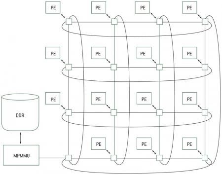
The system (Figure 1) is composed of three basic elements:
Figure 1
Medea – an illustrative configuration
- an on-chip network;
- processing elements and their interface to the NoC; and
- the multiprocessor memory management unit (MPMMU).
NoC infrastructure
The NoC infrastructure is based on a two-dimensional folded torus topology. Intrinsically, 2D networks such as meshes and tori optimally suit silicon implementations.
With regard to the network routing strategy, switches implement a deflection-routing algorithm that uses a full-blown packet-switching methodology by allowing different routing for every flit of the same packet. The basic idea is to choose the ‘best’ route for each incoming flit, without ever keeping more than one flit per input channel (hence this technique’s alternative name, ‘Hot Potato’ routing).
This type of adaptive routing does not suffer from deadlock although livelock may occur in theory. However in previous work [1], we observed sporadic cases of single flits delivered with high latency that did not significantly hamper execution times. In Medea’s specific case, we also did not observe any overhead due to significant excess of latency.
Another advantage of deflection-routing is the small area of the switch. Its storage requirements are at the theoretical minimum (as much memory as the incoming flits), no bottleneck is created by long packets as in wormhole routing, and no back-pressure mechanism is needed. The trade-off here is the introduction of a potentially out-of-order reception of flits belonging to the same packet at a destination.
Processing element and NoC interfaces
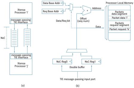
The Tensilica Xtensa-LX configurable processor was used to implement the MPI message-passing interface as a high-speed direct link between each processor and the switch using TIE (Tensilica Instruction Extension) ports. This I/O directly connects to the processor register file and behaves as a FIFO queue interface (Figure 2a).
Figure 2
A FIFO-like IPC model and details of the receiving interface
When a packet of length L flits must be sent, the interface puts a sequence number into all flits. An address in the form XY is put in as well. To speed up the operation and achieve maximum throughput for a flit per cycle, an additional counter for the sequence number and a LUT for addressing has been instantiated within the processor core and supported by custom TIE instructions. The sequence number is used at the receiver to avoid any buffer for sorting flits received out of order. When a flit arrives, the PE first reads a flit from the NoC, storing it in a register, and then uses the sequence number of the given flit as an offset address for storage into the processor data memory. Another register contains the base address. A double buffer technique enables one clock cycle read operations (Figure 2b).
Figure 2
A FIFO-like IPC model and details of the receiving interface
The size of the sequence-number field determines the size of the logic packets. Additional hardware consists of a small adder and two registers, which are seamlessly integrated by Tensilica core development tools in the processor pipeline. The choice of embedding the interface in the processor allowed the ISA and consequently the compiler to natively support all message-passing I/O thus facilitating the development of an ad hoc scalable programming model. This is mandatory because scalability of the hardware infrastructure must be fully supported by software layers.
Gate count overhead is around 5,000 for a 64-bit wide flit. The shared-memory interface between the processor and the NoC has been implemented through the pif2NoC bridge, which translates the Tensilica PIF protocol bus transactions to a sequence of NoC flits. The bridge can perform single read/write operations as well as block transfers. The translation of a shared-memory address into an NoC address depends on a configuration memory inside the bridge and can be directly configured by the microprocessor. In the simplest implementation, all the memory-mapped address space is located at the unique MPMMU of the system (even if there are no limitations in the number of MPMMUs) thus the corresponding NoC address is hardwired. This reflects the choice of a single physical memory node. In every block-read transaction, the different flits containing words read from the MPMMU may arrive out of order. Block reads are common during cache misses. The current processor configuration supports a cache line of 16byte, so a miss causes a block read of four 32bit words. For this reason, the pif2NoC bridge contains a reordering buffer with a depth of four words. Access to the NoC from the different interfaces, message-passing and shared-memory, is guaranteed by a simple, configurable arbiter.
Three configurations are possible depending on required system performance and area availability.
- The two interfaces connect to the NoC with a simple multiplexer and no buffers. In case of contention, one interface receives access to write to the NoC while the other waits until the resource is released.
- A single FIFO is available. So even if the switch connected to the given processor cannot accept other packets due to congestion, the two interfaces can store packets in the queue.
- Two FIFOs are used: one for ‘high-priority’ and one for ‘best-effort’ traffic. The arbiter reads the best-effort queue only if the high-priority one is empty.
Since the architecture can be used for scientific computations, double precision floating point acceleration has been incorporated.
MPMMU
The MPMMU handles shared-memory transactions (reads/writes) using a protocol defined by the authors. It has one NoC interface (the TIE ports) and a PIF bus connected to a double data rate (DDR) controller. The MPMMU can be seen as a slave—it always answers to transactions initiated by other processors. The NoC interface uses two FIFOs for incoming packets and one FIFO for outgoing packets. Incoming packets can be of Pif- Requests/Control or Pif-Data type.
The Pif-Request/Control FIFO receives ‘request-for-transaction’ tokens generated by cores and performs read/write (single/block) shared-memory transactions. The depth of this queue is as large as the number of processors. The token contains the source-ID of the transaction, memory address and type of transaction. For a write request, the MPMMU issues a grant to the sender. Incoming data is stored in the Pif-Data queue, read by the MPMMU and stored in memory. Finally, a second acknowledge is sent to the transaction initiator. For a read request, the MPMMU sends requested data immediately using the outgoing FIFO. The Request/Data protocol has been implemented to provide an implicit flow-control scheme that minimizes local buffers in the MPMMU.
The global shared-memory is divided into two logic segments, a shared and a private area. A system with N cores will thus have N private segments and one shared segment. Since the private area can be accessed only by one processor, no coherency is required between the L1 cache of that processor image of the private segment on the system memory. To support atomic operations such as critical sections, a lock/unlock mechanism of a given word in shared-memory has been implemented. Every processor which aims to access the shared memory segment must first request ‘lock’. If granted, the line can be read/written. Before ‘unlocking’ a line, the processor must perform an L1 cache flush operation on it to maintain coherency. All the lock and unlock requests are stored in the Pif-Requests/Control queue.
Network protocol
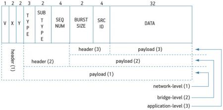
The system network protocol can be divided into three levels: transport (network), bridge and application (Figure 3, p. 20).
Figure 3
Three-level packet-format description of the Medea architecture
The transport-level is used by NoC switches to route flits through the network, requiring only the destination address expressed as X–Y coordinates and a validity bit. The destination address field depends on network size. For a 4×4 folded-torus topology two bits are required for each coordinate. A pif2NoC bridge supports memory-mapped transactions, thus some extra fields are required (type, sub-type and sequence-number).
- The first one is a three-bit field and expresses seven types of packet (single-read, single-write, block-read, block-write, lock and unlock for shared-memory transactions, and one for generic message-passing packets).
- The sub-type field is a two-bit field used in shared-memory transactions to define whether the given packet is an Ack/Nack or has an Address/Data in the payload. For a message-passing flit, it is used to distinguish requests from generic data packets.
- The sequence-number is a four-bit field. It is used at the receiver to perform the re-ordering process of incoming packets in case of out-of-order delivery. The pif2NoC bridge has an internal reordering buffer with depth of four elements in the current implementation. The TIE message-passing interface has internal hardware, supported at instruction-level, that uses the sequence number as an offset to properly store incoming packets in memory.
All the protocol fields of the application level are written and used by the software layer. Source-ID and burst-size are examples. The source-ID is four bits while the burst-size, two-bits wide, is used by the receiver and indicates how many flits belonging to the same logic packet to expect.
Programming model
At startup, code to be executed is placed in an external DDR memory. After reset, all processors start to fetch initialization routines. If a processor accesses its own private segment located in system-memory, no particular precautions are necessary to maintain cache-coherency. Thus, this segment is completely cacheable. More attention is required for shared-data.
First, shared-data structures must be placed in the shared-memory segment and declared as volatile to alert the compiler that this structure has potential side effects.
Second, when the producer wants to write data in this shared segment, a cache flush of the line must be performed to make sure that coherency exists between the local L1 cache and the global system-memory. Also, the consumer of a given data in the shared segment must avoid incoherency making its address uncacheable.
For small memory regions the DII instruction can be used to invalidate a specific address of the cache thus forcing a fetch from the system memory. For wider segments of at least 512MB it is better to define the entire segment as uncacheable, bypassing the cache mainly where there are frequent accesses.
For the message-passing model, we implemented a subset of MPI APIs, embedded-MPI (eMPI). With three basic primitives—MPI send(), MPI receive() and MPI barrier()—direct communication between cores is possible, often totally avoiding access to the global-memory. These high-performance I/O primitives can be used for synchronization between cores as well as for data exchange. The best conditions arise when data to be sent completely reside in the local L1 cache.
Results
Cycle-accurate SystemC models of architectural blocks were developed along with their RTL versions. Tests for compliance as well as speedup were run against an HDL-ISS cosimulation. On average, we achieved a speedup of 15x and a perfect overlap of behavior. Such simulation speed enables accurate design space explorations for many candidate architectures in hours, compared to days needed for HDL-ISS equivalents.
We had to select a benchmark that could stress both the computational and the communication resources. Such applications had to be scalable according to the number of processing elements as well as memory size in such a way as to keep a constant level of pressure on systems with different characteristics.
The chosen algorithm was an iterative solver for 2D partial differential equations. It can be shown that the Jacobi algorithm [2] is a solver for this class of problems. We were able to run a parallel implementation of the algorithm for three different sizes of input data on 168 different architectures in about one day. Some 168 points in the design space were obtained by varying the number of cores between 3 and 16 (one being the MPMMU), varying cache size between 2kB and 64kB (scaled according to the power of two), and using a Write-Back and Write-Through cache policy.
The Jacobi algorithm was run on 16×16, 30×30 and 60×60 double-precision floating-point arrays. The three sizes, though relatively small, compared to a large Jacobi problem solved by a cluster of hundreds of nodes. The smallest case was dominated by communication cost whereas the performance of the largest was dictated by computational cost. It was clear that a system optimally configured for the hybrid approach (cache size and core number) was not optimal for the purely shared-memory approach in terms of number of cores.
A Write-Through policy makes it easier to keep caches coherent, but shows poor performance due to an excessive amount of traffic. For the Write-Back case, communication cost due to a high miss rate almost dominates for a cache size of less than 8kB, leading to a small speedup or no speedup at all. When the amount of data per core fits in the cache size, computational costs emerge that clearly scale with the core number.
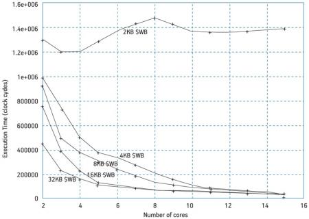
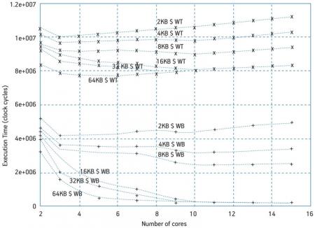
The curves in Figure 4 (p. 20) are representative of the type of system data the simulator can present to the user. In this case, plots represent execution time in clock cycles for an iteration of the Jacobi algorithm after cache warm-up as a function of the number of active processors (2 to 15) and varying the cache size. The data size is 60×60.
Figure 4
Execution time for a 60×60 array varying number of cores, cache size and cache policy
Figure 6 reports execution time for the 30×30 case, write-back only. Scalability is hampered if caches are not properly sized. In the 30×30 case cache must be at least 4kB large, a value 4x less than the larger 60×60 case because the array is 4x smaller here.
Figure 6
Execution time for a 30×30 array varying number of cores and cache
That last remark concerning area (and, as a related variable, power consumption) is important for cost-effective or power-constrained multicore implementations. In general, a good rule of thumb allows an increase in resource size only if for every 1% increase in core area there is at least a 1% increase in core performance (the ‘kill’ rule [3]). We accordingly pruned the explored solutions that were Pareto-dominated (larger area for a smaller performance) and kept only those that resulted in a performance increase at the minimum cost.
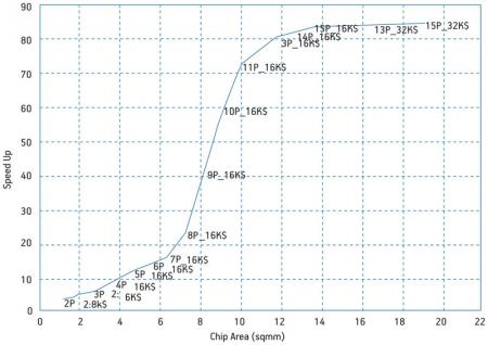
The resulting ‘optimal speedup’ is plotted in Figure 5 (p. 21) for the three cases of data size as a function of chip area. The latter was estimated from core/cache data given by Tensilica for a TSMC 65nm CMOS technology and including overhead for NoC switches, bridges and a routing area of about 100% of the total core area (excluding caches). Labels along the curves describe the processor/cache configuration that corresponds to the optimal (area, speedup) point of the curve to which the label is attached. The first reported case concerns the bigger data size case.
Figure 5
Run on a 60×60 array: optimal speedup and corresponding architecture configuration versus chip area
It can be correlated with the curves in Figure 4, which show that execution time decreases in the 4-10-core range faster than in the 11-15 range. This corresponds to the upper knee of the optimum speedup curve. The 11-processor pool equipped with 16kB L1 cache each is the limit beyond which increasing area any further did not produce a proportional performance increase. As for the lower knee, the speedup abruptly increases when the amount of data for each processor fits in a 16kB cache. In the range of 7-10mm2 area, the speedup increase is (70-20)/20=2.5 for an area increase of (10-7)/7=0.43. The 8-11 grouping is therefore the range of processor cores that will lead to an ‘optimal’ design in the sense that it best exploits the available area.
Figure 4
Execution time for a 60×60 array varying number of cores, cache size and cache policy
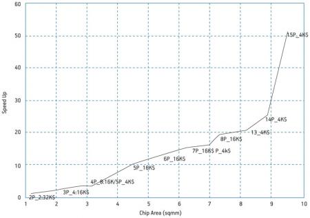
For theoptimal speedup for the 30×30 data size (Figure 7, p. 23), we can observe similarities in what happens at the lower knee of the curve for a 4x lower cache. However, these results are also observable, somewhat unexpectedly, for a larger number of cores. The upper knee and so the limit of the kill rule would probably occur for a number of cores greater than 15. Below the lower knee, the optimal cache size is larger than 4kB, an indicator that miss-rate dominates in that range.
Figure 7
Run on 30×30 array: optimal speedup and corresponding architectural configuration versus chip area
To understand and quantify the advantage of the hybrid shared-memory/message passing approach, we redesigned the Jacobi code in two ways: a pure shared memory and a hybrid version where only synchronization uses message-passing primitives while data exchange occurs through the shared memory. We expect that the amount of traffic generated toward the memory as well as the serialization of accesses will degrade the performance in both cases, but it is important to understand how much of the speedup will be due to synchronization and how much to data exchange. Given a 60×60 array, we compared the optimal speedup of Medea reported in Figure 5 to the pure shared memory case and observed a 2x improvement of Medea below the lower knee and an increasing gap beyond the knee ranging from 2x at six processors and 16kB cache to more than 5x at 10 processors for the same cache size. This behavior confirms expectations. When the traffic generated by the miss-rate is relevant in the Medea case, the results are still better than the shared memory case in which, even in the absence of miss rate, traffic is always present.
Figure 5
Run on a 60×60 array: optimal speedup and corresponding architecture configuration versus chip area
The difference, however, is not as dramatic as where memory accesses beyond the L1 cache are nullified in the hybrid case. In the same conditions, we evaluated the speedup when both data and synchronization exchanges occur through message-passing with respect to the case in which messages are sent for synchronization only. In the same range in which the speedup was 2x compared to the pure shared-memory case, the speedup was similar (only 2-20% smaller). When the miss-rate was negligible, the speedup ranged between 2x and 2.8x instead of 2x and 5x. We can thus state that much of the improvement of the full-blown message-passing approach was due to better synchronization accounting for at least 100·2.8/5=56% of the record 5x improvement that we mentioned above and up to 100% of the 2x cases. As a partial conclusion of this analysis, the hybrid approach—in both its variants, synchronization only as well as data-plus-synchronization case—seems to scale better and to exploit the silicon area for additional core instances in a more efficient way compared with a standard shared-memory approach. Cache size is a critical parameter: When the miss-rate becomes relevant, the advantage fades away.
References
[1] S. V. Tota, M. R. Casu, L. Macchiarulo, “Implementation Analysis of NoC: A MPSoC Trace-Driven Approach”, Proc. ACM Great Likes Symposium on VLSI, Philadelphia, April 30-May 2, 2006.
[2] G.E. Karniadakis et al., Parallel Scientific Computing in C++ and MPI, Cambridge University Press, 2003.
[3] A. Agarwal et al., “The KILL Rule for Multicore”, Proc. Design Automation Conference, 4-8 June 2007, pp.750-753.
Dipartimento di Electtronica
Politecnico di Torino
Corso Duca degli Abruzzi
10129 Turin
Italy
W: www.infotech.polito.it
