Improving performance through better delay estimation of sub-32nm interconnects
Better delay estimation of sub-32nm interconnects, in which resistivity varies up to 100x between layers, helps Cavium improve overall performance and get ready for even denser processes
At 32nm and below, metal resistance varies significantly (~5X-100X) between routing layers, providing both challenges and opportunities for accurate interconnect delay estimation. To minimize design costs and better predict system performance, more accurate pre-route parasitic estimation of interconnects is necessary. In this article we review IC Compiler’s layer-aware optimization technology, which uses an understanding of resistance variation between layers to enable better performance prediction. Cavium demonstrates the use of this technology to meet aggressive performance and schedule targets.
Introduction
A recent Synopsys user survey showed that more than 50% of designers are working at the 32nm node and below, implementing large designs with fast clock frequencies [1]. At emerging nodes one of the challenges is the increase in interconnect length as shown in Figure 1. With longer interconnects, wire delays begin to dominate gate delays. The shrinking feature size reduces gate delays significantly but have the opposite impact on interconnect delays.
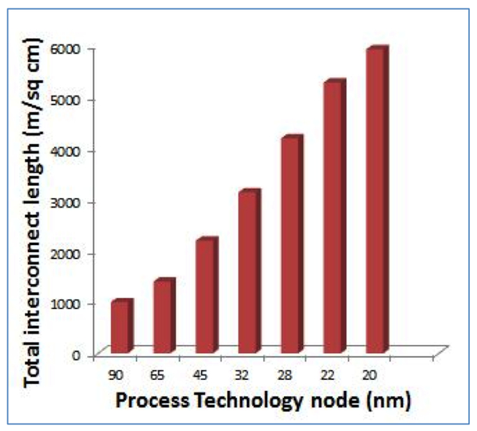
Figure 1 Total interconnect length has been doubling from 65nm to 32nm to 20nm (Source: ITRS)
The increase in interconnect delays is due to:
- Metal layer structure: Wires are getting thinner and the spacing between them is decreasing, resulting in increased interconnect delays.
- Increase in the number of metal layers: To meet integration needs, emerging technology nodes come with an increasing number of routing metal layers. The number of metal layers has approximately doubled every decade, reaching a current maximum of 12.
- Non-uniform pitch across metal layers: At emerging nodes, the metal pitch varies from narrower widths for the lower layers to wider widths for the upper layers. Layer-width variation results in lower metal layers having more routing resources but at a higher resistance and upper layers having fewer resources but at a much lower resistance. At the 40nm and 28nm process nodes, the metal stack exhibits ~5X-100X resistance variation between metal layers [2].
These issues must be taken into account during the pre-route parasitic estimation of emerging node designs. If they are not addressed, they can pose a serious challenge to meeting quality of results (QoR) and schedule objectives.
Pessimistic delay estimation and ways to address it
While implementing a sub-32nm complex system on chip (SoC), Cavium experienced several design challenges including weak correlation between pre and post-route delay estimates, as well as too much (or too little) buffering on certain nets. These challenges were linked to the large resistance variation across the metal stack, as shown in Figure 2.
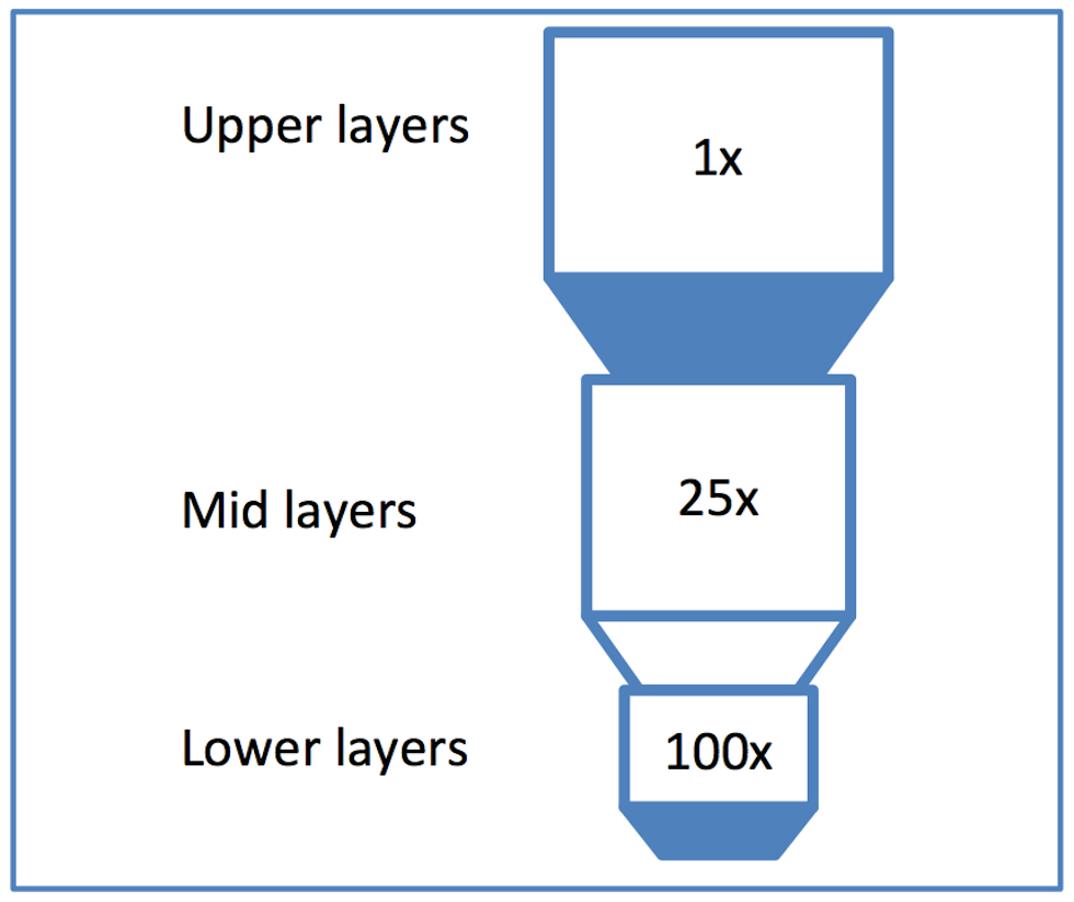
Figure 2 Metal stack with large resistance variation between layers (Source: Synopsys)
Pre-route optimization typically uses an average resistance of all the allowable routing layers to calculate parasitic delays. This works well if the metal layers exhibit uniform resistance. At the post-route stage, parasitic delays are calculated based on detailed route topology, and the actual resistances of the metal layers used. With the large resistance variation in the metal stack, Cavium noticed that layer averaging during pre-route made the delay estimates for longer nets pessimistic and those for shorter nets optimistic. This resulted in increased buffering and cell upsizing for longer nets, and vice versa for shorter nets. This in turn led to correlation issues as long nets that span the chip were over-buffered, while short nets were under-buffered. This affected timing, area, power and routability, and delayed design closure.
The challenge of correlating pre- and post-route delay estimates due to non-uniform layer metal stacks is well understood. Before layer-aware optimization was supported in P&R tools, Cavium designers manually applied layer constraints on critical nets to meet timing – an iterative and time-consuming process. Layer constraints had to be applied at every stage of the flow, and designers had to keep track of the net name changes at each optimization stage and update the layer constraints accordingly.
Layer-aware optimization technology: Cavium’s approach
Cavium designers needed a more automated and predictable approach to address these correlation challenges. They were aware of the unique characteristics of their designs and understood that to fully utilize layer-aware optimization, they would need to develop a flow that matched their design objectives. The team formulated a three-pronged approach using IC Compiler layer-aware optimization technology:
- Develop intelligent net selection criteria to exploit the large resistance variation across metal layers
- Use more accurate pre-route RC estimation for better correlation and routability
- Make the flow reusable and minimize the turnaround time (TAT)
It was a challenge to identify the critical nets to be promoted to the upper metal layers. There were many options available for net selection including net length, fan-out, area, slack threshold, IO connections, and more. Defining the right criteria was important; if too many nets were selected for promotion to higher layers, it could cause congestion and routability issues. On the other hand, if too few nets were promoted it could lead to correlation issues as well as routability issues on the lower routing layers. To avoid this, the designers selected nets based on two criteria: timing criticality and length.
- Timing-critical nets were identified based on slack
- Long nets that were likely to be over-buffered during pre-route were identified based on a maximum-length threshold
While timing slack was the main criterion for applying layer constraints, to avoid congestion on the upper layers it was not used on all violating nets. Cavium used a carefully chosen factor, based on slack and the number of violating paths within the slack range, to promote nets above a threshold to the upper layers. This gave Cavium a way to control the number of nets that were assigned to upper layers and so avoided congestion. With this approach, many nets with high negative slack were promoted to layers with lower resistance to meet timing. A few violating nets remained that were below the slack threshold and hence were not promoted. Cavium uses built-in margins in the implementation flow, which makes timing more pessimistic during P&R. These margins are removed during signoff, reducing the remaining number of violations. For some outliers, engineering change orders (ECOs) fixed the violations, either through cell sizing, or by swapping a small segment of the net to a higher metal layer.
Implementation methodology
The design team developed an implementation methodology based on the IC Compiler layer-aware optimization technology, as shown in Figure 3. Layer optimization constraints, once defined based on user guidance, are automatically converted by IC Compiler into non-default rules (NDRs) and stored in the Milkyway database. As the design goes through clock tree synthesis (CTS), post-CTS timing optimization and detailed routing, IC Compiler tracks changes to the nets and their names, so that there is no need to redefine these rules multiple times.
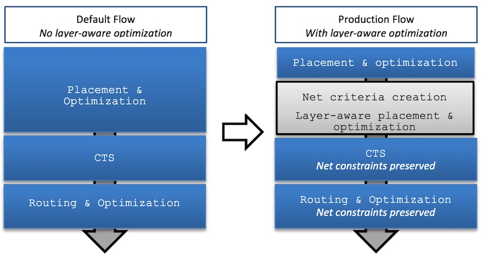
Figure 3 Layer-aware implementation methodology (Source: Cavium)
With the deployment of this implementation methodology, Cavium was able to meet key design objectives, as shown in Table 1.
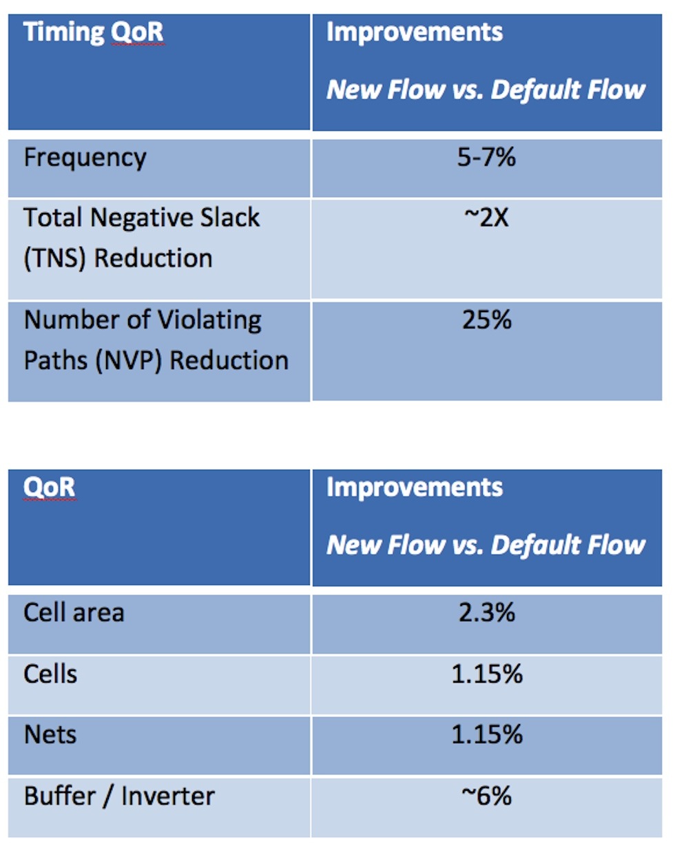
Table 1 Layer aware optimization significantly improved QoR (Source: Cavium)
Besides the expected QoR benefits of improved clock frequency, reduced buffer count and gate area, Cavium also saw TAT benefits in terms of fewer ECOs and faster design convergence, which helped meet their aggressive design schedule.
Conclusion
At 32nm node and below into the emerging FinFET processes, metal resistance variation across routing layers provides challenges and opportunities. In this article, Cavium has shared their successful use of IC Compiler layer-aware optimization technology to meet aggressive performance objectives and schedule targets.
The next step in Cavium’s quest to improve pre- and post-route correlation is to evaluate IC Compiler’s global-route based pre-route optimization capability, along with its global-route based layer promotion.
Authors
Susheel Sharma is a consulting engineer at Cavium working on physical implementation of complex chips in latest technologies. He has over 20 years of experience and has held engineering and management positions at STM, Avanti, Synopsys. He holds a Master’s in Electrical Engineering from Santa Clara University, CA and MBA from India.
Jafar Safdar is a product marketing manager for IC Compiler at Synopsys. Over the past 18 years, he has held various application engineering and marketing positions at Synopsys. He holds a master’s in electrical engineering from California State University Northridge, CA, USA.
References
[1] Synopsys Global User Survey 2012
[2] G. Rangarajan, “Design How-To: Layer-aware optimization”, EE Times, 8/27/2012
Company info
Cavium, Inc.2315 N.First Street,
San Jose, CA 95131
Telephone: +1-408-943-7100
Fax: +1-408-577-1992
Email: info@cavium.com www.cavium.com Synopsys Corporate Headquarters 700 East Middlefield Road Mountain View, CA 94043 (650) 584-5000 (800) 541-7737 www.synopsys.com
Sign up for more
If this was useful to you, why not make sure you’re getting our regular digests of Tech Design Forum’s technical content? Register and receive our newsletter free.