Better PCB design using the fabricator’s view
Early use of design for manufacturing can capture PCB yield issues related to pads, copper distribution, same net slivers and more
PCB designers can get so deeply immersed in their work that they hardly consider manufacturing. It can be difficult to see the forest for the trees. Adopting another perspective — that of fabricating and populating the PCB — can help make a product much easier to assemble and improve overall quality.
Fabricators consider a design in terms of aspects that can affect yield, cost and delivery. So, let’s take ‘the fabricator’s view’, and extend our understanding of what they do with design data to produce a board within their constraints. We’ll use a typical PCB production process to highlight design for manufacturability (DFM) techniques that can be used before a product goes to fabrication.
DFM anticipates issues the fabricator normally checks later in the flow. Because the rules and processes are quite extensive, many PCB designers use DFM tools such as Mentor Graphics’ Valor NPI software to perform these extensive checks. It gives them the assurance that a design will reach target production quickly and not require major rework.
The PCB fabrication process
Figure 1 summarizes the PCB fabrication process for standard, multilayer boards (we will later discuss issues specific to microvia technology).
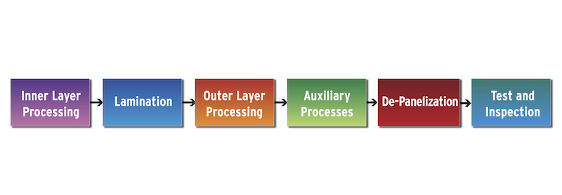
Figure 1
A specific set of DFM rules maximizes yields for each process step (Source: Mentor Graphics – click image to enlarge)
On multilayer PCBs, the inner layers are processed first, then laminated together for outer layer processing. Next, come several steps we label ‘auxiliary processes’, such as solder mask application. The fabricator will finally de-panel the PCBs and finish with test and inspection. We’ll follow this sequence as prompts for a few important rules can will help determine if a design can be fabricated at high yields. In reality, though, there are more than 270 rules that can be used.
Inner layers
The first step in processing inner layers is dry film preparation and inner layer coating.
The copper foil is coated with a thin photoresist film. The inner layers are then be placed into the imaging system and both sides exposed either with a conventional film plotter or a laser direct imaging system. Next, the layers are developed so that the unexposed photoresist is washed away. The PCB fabricator then etches away the unprotected copper and the protective coating on the circuits is stripped.
At this point, the fabricator will typically determine if a pad and a circuit are too close (Figure 2) and may bridge during imaging, etching, plating, or soldering and result in a short circuit. One reason why this can happen is that all fabricators have to add a global etch compensation to the circuitry. This is so the copper features end up as designed after etch. Moreover, the amount by which they grow those features depends on what weight of copper the design requires. A PCB design using half-ounce copper requires much less etch compensation than one using two-ounce copper. In applying the etch compensation, the fabricator risks making the spacing between two circuits too close, and creating the opportunity for a short.
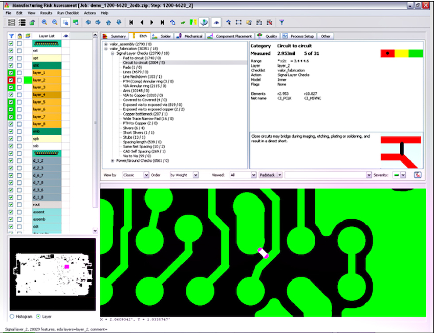
Figure 2
Pads too close to a trace on an inner layer are serious errors and must be fixed (Source: Mentor Graphics – click image to enlarge)
Floating planes raise another issue. These copper areas are often used as reference planes that have become disconnected. Locating them minimizes the likelihood of a critical net losing its reference plane, or even worse, losing an electrical connection and creating an open net. The issue is most frequently seen on negative planes because of how they are displayed and output by CAD tools, but they can occur on positive planes as well. The opposite can also occur. When spacing between planes is compromised, shorts can occur between different voltage sources or between power and ground, resulting in nonfunctional boards.
A further concern can be the insufficient connection of a plated-through hole to a plane if it is not completed within the desired plane area. This can be missed by the CAD tool as it shows it as still connected electrically. When the hole is plated, it will not have a full connection to the plane, and will therefore be subject to failure. The DFM rule values can be set as a percentage of overlap to the plane required to assure a solid connection.
Finally here comes insufficient thermal connection. Since the purpose of thermals is to concentrate heat into the barrel of the via for proper plating, the thermal connections to the plane must be sufficient for this heat distribution. In instances where all four spokes are reduced to a very small connection to the plane, there is a real risk of in-the-field failure as these vias will have poor plating within them.
Lamination
During lamination, the inner layers are treated with an oxide to inhibit corrosion and help ensure proper adhesion during lamination. During ‘booking’, the fabricator lays out the materials that will constitute the full PCB. Panels are pinned followed by inner layer cores and prepreg layers. Then the copper foils for the outer layers are stacked up according to the recipe. Fabricators often stack up to four panels in one ‘book’ at a time in the lamination press for greater efficiencies. The panels are placed between two metal plates in the press where pressure and heat are applied for several hours.
Ideally, all layers will have a good distribution of copper throughout the design. This is most critical for thin-core PCBs. Additionally, the fabricator is going to pay close attention to the copper distribution on outer layers for plating purposes. Poor distribution will make it very difficult to achieve a consistent plating quality.
Figure 3 shows a PCB copper distribution. Red represents high density areas; blue represents areas that lack copper. This information, along with the copper versus non-copper percentage, helps the fabricator determine and apply pattern fills to evenly distribute the copper as necessary for optimum plating.
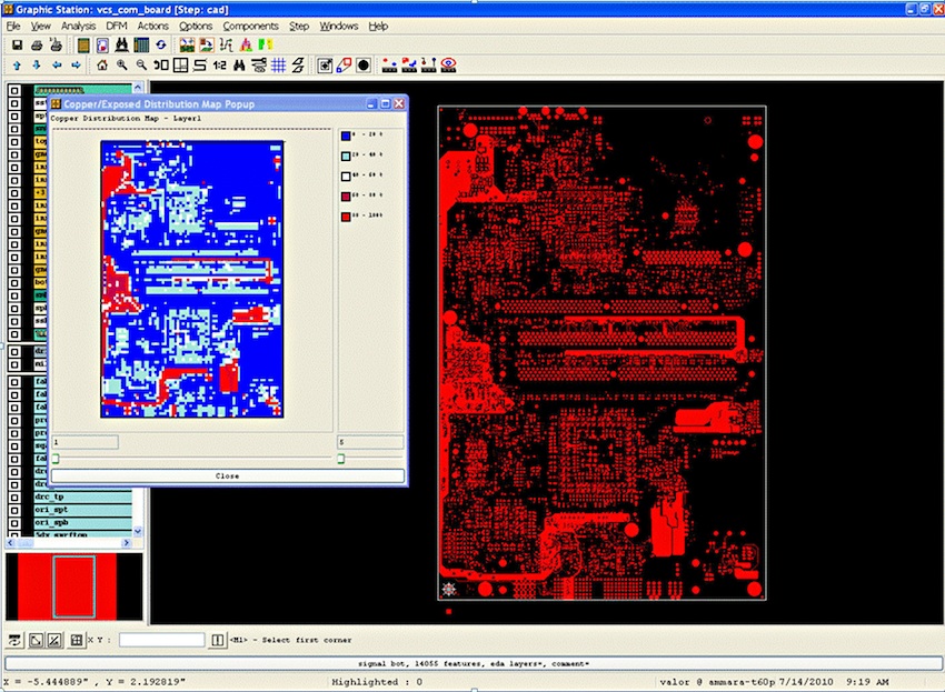
Figure 3
Copper distribution under DFM verification. Uneven distribution can warp boards or compromise plating (Source: Mentor Graphics – click image to enlarge)
Drilling is another important consideration. In addition to the material registration tolerances on a multilayer board, the layers move in a nonlinear manner when in the press. This can influence drill alignment. Vias that may have been well aligned before lamination may be only marginally aligned after.
Moreover, fabricators often stack and drill multiple PCBs to save cost. This means that minimum annular rings must be checked. Furthermore, the correct annular ring varies, depending on whether the via is mechanically- or laser-drilled. Mechanical drill bits bend slightly as they penetrate copper layers. For very dense designs, designers strive for the smallest annular ring possible, as less space is taken by the pad or via and more space can be dedicated to routing traces. However, taking the annular ring constraint lower can have a great impact on cost and yield during fabrication. So there are tradeoffs involved and DFM informs the designer on how to make the best decision.
For designs incorporating microvias, fabricators determine the depth by which a microvia (or combination of overlapping microvias) penetrates the layer stack-up as that can affect yield. The greater the number of layers penetrated by overlapping vias, the more prone the microvia is to hole fracture.
Outer layers
The laminated panel is now ready for outer-layer processing. As during inner-layer processing, photoresist film is applied to each side, and the panels undergo either film or laser direct imaging. Inner layers that are typically negative images, but outer layer imaging is done with positive ones. This is because the circuit image on the photoresist is developed away, leaving the circuit copper exposed for plating.
Most PCB tools let you define unique constrained areas within a PCB. A good example is those for BGAs, where you want to have much tighter rules than apply elsewhere. DFM software should read these CAD-constrained maps. This saves the user manually reviewing all the ‘false’ DFM violations caused by using general PCB rules within those constrained areas.
One common violation on outer layers is a ‘same net sliver’ (Figure 4). While electrically correct, these present significant difficulty to the fabricator. In cases like that illustrated, the width of the photoresist (in black) is so thin it runs the risk of breaking and then redepositing elsewhere, potentially leading to a short or an open. Today’s strict and low tolerance constraints for high speed nets mean same net slivers can shorten connections and significantly change circuit impedance.
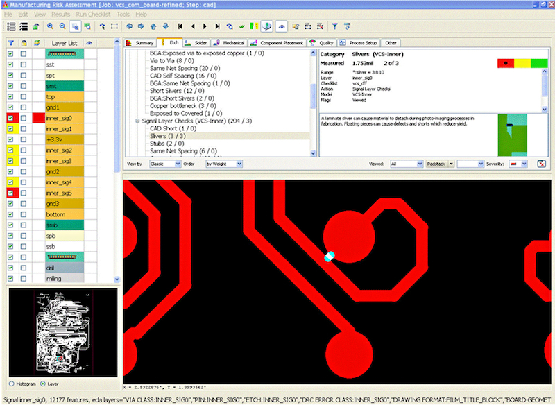
Figure 4
A same net sliver can cause a short or alter the connection impedance (Source: Mentor Graphics – click image to enlarge)
Final processing
Final PCB processing begins with the application of solder mask and silkscreen. Typical solder mask checks include rules that govern how closely lines can pass to a pad and how close two pads can be.
Lines that pass closely must be fully covered by mask to avoid solder bridging between the line and pad. If we again consider process tolerances, the application of photo-imageable solder mask has a positional tolerance of +/- 3 mils or .08 mm. It is important that you have at least this much clearance around your solder mask pads.
DFM can also identify very small slivers of solder mask between two pads. If a piece of mask detaches, the cause is typically a bad solder joint that has resulted in mask debris becoming embedded in the solder. This can cause a bad connection or even an open depending on the size of the mask fragment compared to the size of the joint. Below a minimum web width of around 0.1 mm, the fabricator must use a gang solder mask.
These issues may not be identified at the design stage because many PCB designers follow IPC’s recommendation to create solder mask 1:1 with the pad. The idea is that the fabricator will add the necessary growth to the mask for its process. However, by ignoring this at the design stage, you run the risk that these solder mask issues, once found by your fabricator, will cause a delay while you change the layout or approve the use of a gang mask.
Silkscreen can cause other problems. It should never be applied on pads because it is considered a solder contaminant and will prevent the formation of a quality joint. If the defined silkscreen uses a stroke size too small for the screen printer to image, it is probably too small to serve its purpose. The fabricator will consequently seek permission to increase the line width or to remove it from the legend. Although this may not be a fatal error, it is another possible source of delay.
One last step remains before test. The fabricator separates the panels into individual PCBs and makes all internal cutouts or routs. Here the design must maintain a minimum copper setback from board or slot edges to avoid damaging the circuits. Keep in mind that most CNC routing is going to have a mechanical tolerance of +/- 10 mils or .25 mm.
Conclusion
Without good DFM verification practices during design, many of these issues will arise as the board now goes to electrical test, carried out with a flying probe or flying grid tester for low volumes or with a bed-of-nails tester for higher volumes.
The more aware you are of your fabricator’s perspective, the fewer issues you will have once you release your PCB design to manufacturing. Do not to wait until your fabricator discovers these problems but use DFM verification software during the design process so that your fabricator will be just as happy with your design as you and your layout tool.
About the Authors
Ammar Abusham is a Senior Applications Engineer at Mentor Graphics. He has been involved with Design for Manufacturability solutions for more than 12 years.
Patrick McGoff is a Market Development Manager, who joined Mentor Graphics as part of the acquisition of Valor. During his fourteen years at Valor, he held various sales and sales management positions, including VP of Sales for North America, VP of Sales for China and Director of Sales, Strategic Accounts.
Contact
Mentor Graphics
Corporate Office
8005 SW Boeckman Rd
Wilsonville
OR 97070
USA
T: +1 800 547 3000
W: www.mentor.com

really Good .Its very important points at the time of Layout and footprint creation for SMD components