Implementing USB Type-C
A look at three design challenges for USB Type-C: implementing two SuperSpeed datapaths on a reversible connector; partitioning the design to support multiple USB Type-C variants; and partitioning the management software.
USB is a widely used interconnect standard, and the introduction of the USB Type-C connector will make it even more so. The USB Type-C connector is small, is used at both host and device ends of a cable, and can be plugged in either way up. It can deliver simultaneous power (with a local power source), data, video, and audio, for example in docking applications.
There are three challenges in designing support for USB Type-C connectors:
- Implementing two SuperSpeed datapaths on a connector that can be used either way up.
- Partitioning the design to support multiple variants of USB Type-C. This can involve creating precision analog circuitry as well as high voltage/high current switches, which may be implemented as discrete components, in dedicated USB Type-C controller chips, as part of a power-management IC, or within the SoC.
- Partitioning the USB Type-C management software to run on a main processor, internal microcontroller, microcontroller in a power-management IC, or an external dedicated USB Type-C chip.
Datapath implementation
The USB Type-C connector is symmetrical and duplicates many signals so it can be used either way up.
Figure 1 USB Type-C pinout and rotational symmetry (Source: Synopsys)
This requires datapath multiplexers for SuperSpeed USB products, and datapath crossbar switches for Alternate Mode products. Designers can achieve this four ways:
External datapath switch
External datapath switches (or multiplexers, see Figure 2) are already available, based on high-frequency analog switches designed for PCIe, Ethernet, SATA, and DisplayPort. The disadvantages of using them are cost, PCB area and possible signal degradation.
Figure 2 Logical model for data bus routing across USB Type-C-based ports (Source: Synopsys)
Loss in the switch affects the channel loss budget from the USB port to the Type-C connector. For USB 3.0 implementations, this can limit the length of PCB traces from USB port to connector to around 15cm, depending on the quality of the PCB.
For USB 3.1 implementations, which have a smaller channel loss budget, the use of an external switch can cut PCB traces lengths to 5cm or less.
Two PHY or two-port solutions
The quickest way to implement an SoC with USB Type-C support is to use two USB 3.0 or 3.1 PHYs, one of which is active depending on the connector orientation. The other PHY stays in a low-power state. This approach doesn’t use an external datapath switch, so there’s no loss of signal quality, and can more cost effective than an external switch or switch and redriver.
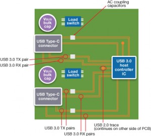
To build multiport USB hosts, two existing Standard-A ports can be used to create one USB Type-C port. Figure 3 shows a common 4-port USB 3.0 host controller being used in a 2-port USB Type-C host controller plug-in board. Two SuperSpeed USB RX and TX pairs are used for one Type-C connector. To preserve signal integrity, the SuperSpeed signals are routed directly from the controller to the Type-C connector. Two USB 2.0 signal pairs are also routed from the controller to the USB Type-C connector. USB 2.0 PCB routing is less critical and the routing continues on the opposite side of the PCB to avoid interfering with the SuperSpeed USB PCB traces.
The USB Type-C specification requires that Vbus is not enabled until a device is attached. A load switch and capacitor can be seen next to the USB Type-C connector. The host has one Pullup resistor Rp on each CC pin. When a device is connected, the device Pulldown resistor Rd causes the voltage on one of the CC pins to go low. This causes the load switch to enable Vbus. Both ports are active, but only one port detects a device, while the other stays active but unused.
Figure 3 Multiport USB Type-C Host Controller PCB (Source: Synopsys)
This approach is commonly used by laptops with USB Type-C ports. If just one USB controller is used, orientation detection and a datapath switch are still needed.
Internal, on-die switches
An on-die switch has less loss than the external switch, which makes it easier to support 10Gbit/s USB 3.1 Gen2 mode operation, but is difficult to implement because the switch must compensate for non-linear frequency and phase response. The switch must also block crosstalk between high-amplitude DisplayPort and USB TX and low-amplitude USB 3.1 RX signals. Impedance matching is required to prevent reflections.
USB-C PHY
External switches offer the fastest time to market but increase cost, a two-PHY solution uses excessive silicon area, and internal switches are only realistic to implement for USB 3.0. The best solution for SoC integration uses a proven USB-C PHY to reduce risk and silicon area.
Synopsys offers USB-C PHYs for USB 3.0 and 3.1 in advanced process nodes. The DesignWare USB-C 3.1 and 3.0 PHYs are dual-lane solutions, with the same advantages as a dual-PHY solution. These PHYs share circuitry between the two lanes and therefore use less silicon area than a two-PHY solution.
Hardware partitioning
It is not possible to integrate all USB Type-C hardware and features in one multipurpose SoC, so well thought-out hardware partitioning is the key to building cost, power, and area-efficient products using the same SoC.
Although it is possible to integrate many functions on a single die, it can be more cost effective to build different functions in different processes and then integrate the resultant die in a package. Here’s a couple of different ways to make these trade-offs.
Supporting USB Type-C in the PHY vs dedicated hardware
For standard USB implementations, analog audio, UART mode, On-the-Go, battery charging and High Speed USB are all multiplexed on to the USB 2.0 D+/D- pins. This makes it difficult and expensive to use external solutions. The optimal USB Type-C PHY integrates all required functionality into a USB 1.1, 2.0 or complete 3.0 or 3.1 PHY, regardless of process node.
The key challenge for USB Type-C hardware integration is tolerating 5V for high voltage/high current requirements. Even if some of the USB Type-C hardware can be integrated in an advanced process node, external load switches are needed, as well as optional monitoring of Vconn and Vbus. The cost of the extra pins on the SoC and the external circuitry can make this approach less cost effective than using a USB Type-C port controller chip.
The USB Type-C specification gives designers some flexibility with which to address hardware partitioning. The Configuration Channel (CC) pins, used to signal host or device role and host current capability, orientation and Power Delivery Messages(PD msgs), are separate from the USB pins. Circuitry connected to the CC pins detects when a device is attached, which allows products to disable USB functionality to save power. Only one CC wire exists in the cable, so circuitry connected to the CC pins on each side of the cable determines the orientation of the connector.
The Power Delivery aspects of the USB Type-C specification enable up to 100W to be provided from a product over the USB Type-C connector. PD msgs are used to discover voltage and current capabilities, and are multiplexed on CC pins. With these messages, Vbus voltage can increase from 5V to 20V, and current can be increased from a maximum of 900mA (as on standard USB) to 5A.
The CC logic required for USB Type-C products can be integrated in the SoC, but if the solution is expected to support high currents it should be implemented in the power management IC.
USB Type-C port controller interface
The USB Type-C port controller interface (TCPCI) specification defines the hardware and low-level software partitioning for USB Type-C ports. A separate USB Type-C port controller (TCPC) includes the low-level hardware to support CC and PD msg functionality. TCPC can be external to the SoC, integrated within it, or part of a PMIC.
USB Type-C software partitioning
The third challenge in implementing USB Type-C is deciding how to partition multiple variants of product-specific USB Type-C support software. USB Type-C port manager (TCPM) software can be part of the operating system (OS), a product-specific driver module, embedded software in the SoC, or in an external microcontroller.
Support for USB Type-C and alternate modes shouldn’t require changes to the existing USB software stack and USB controller interface.
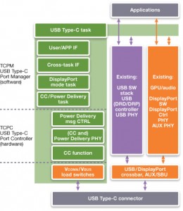
The USB Type-C Port Controller Interface and USB Type-C System Software Interface specifications define high-level USB Type-C software as a separate USB Type-C task, making USB Type-C easier to implement and scale (Figure 6). Many implementation and partitioning choices can be supported without major changes to the OS.
Figure 4 Dividing USB Type-C tasks and responsibilities (Source: Synopsys)
Taking advantage of the TCPCI and USB Type-C System Software Interface specifications should makes software partitioning easier. Keeping USB Type-C functionality in software gives developers more time and flexibility to fix any issues that emerge during development.
USB Type-C Port Manager
The USB TCPM is software than can run on a microcontroller in the TCPC, power management IC or SoC. TCPM can also run on the application processor in the SoC for many types of products.
TCPM can be replaced by advanced TCPC hardware in certain products. For example, a USB 3.0 device will always enable device-mode pulldown resistors, and only connector orientation is detected and signaled to the USB Type-C datapath switch. DisplayPort Alternate Mode products must discover alternate mode capability and then configure crossbar and USB appropriately.
Addressing three USB Type-C challenges
For USB 2.0 designs, existing PHYs can be used with the addition of simple USB Type-C hardware and software. The complexity of this support hardware and software ranges from adding just two resistors to using switchable resistors and voltage comparators, and adapting existing USB OTG software to support USB Type-C.
Synopsys’ DesignWare USB-C PHYs for USB 3.0 and 3.1 are designed to make it easier to implement SuperSpeed USB and SuperSpeedPlus datapaths. Product-specific USB Type-C hardware and software must be implemented outside the USB-C PHY. External TCPC and TCPM products are available until appropriate TCPC hardware and TCPM software is integrated in the PMIC or SoC.
Further information
USB Type-C: what it is and why it matters
USB Type-C: easier for users, harder for designers
Implementing USB Type-C in High-Speed USB Products
Converting Existing USB Designs to Support USB Type-C Connections
Synopsys readies USB 3.1 IP and verification support
Find out more about USB 3.1 and Synopsys’ implementation in its USB University USB 3.1 protocol overview video. There’s also a related white paper, here.
Find out about USB 3.0, which USB 3.1 builds upon, in this series of articles:
USB 3.0 Protocol Layer – Part 1
USB 3.0 Protocol Layer – Part 2
Author
Morten Christiansen is the technical marketing manager for Synopsys’ DesignWare USB IP. Prior to joining Synopsys, he was a principal system designer at ST-Ericsson and Ericsson, designing mobile phone and modem chipsets for 19 years. He was also Member of Technical Staff at ST-Ericsson. Christiansen has contributed to more than 20 USB standards, including USB 3.1, battery charging, HSIC, SSIC, as well as communication standards including WMC, EEM, NCM and MBIM. He has six international patents for other USB inventions. Christiansen holds a Master of Science degree from The Norwegian Institute of Technology.


