Implementing DDR DRAM in automotive applications
A look at how DDR DRAM is being adapted for use in automotive systems, and the demands its use puts upon interface IP for SoCs.
Automotive electronics systems are becoming much more sophisticated as vehicle makers replace electromechanical dials and switches with high-resolution displays, and introduce advanced driver assistance systems (ADAS), such as autonomous emergency braking, as stepping stones to full autonomous driving.
The development of these complex automotive electronics will demand upgraded memory components. Most processors currently used in automobiles have modest memory requirements that can be served by SRAM and non-volatile memory. The shift to high-resolution displays and the introduction of complex computing and image processing to support ADAS features will require the introduction of high-capacity, high-bandwidth DRAM. The question for designers is how to use DRAM in safety-critical automotive systems, especially given its thermal sensitivity, error-rate performance, and the need to meet stringent automotive standards such as ISO 26262.
DRAM vs SRAM in automotive
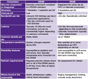
Here’s a comparison (Table 1) of DRAM and SRAM chips in an automotive context.
Figure 1 DRAM vs SRAM use in automotive applications (Source: Synopsys)
DRAM sales are about 100 times those of SRAM chips. DRAM also has a greater capacity and a lower cost per bit than SRAM. In our experience, though, only about 5% of the design wins for DesignWare DDR SDRAM interface IP have gone into the automotive sector, and most of those have been for use in infotainment systems.
Why is this? Here are four reasons:
- Type of computing: The computing needs of safety-critical automobile systems have been modest to date, processing sensor data from the engine, brakes, motion sensors, and driver input to control the engine and braking systems. SRAM has met these computing needs. .
- Lack of camera input and display output: DRAM is often used to support the computing and buffering needs of HD audio-visual input/output, which has been limited to infotainment systems and rear-view cameras.
- Reliability: Some SRAMs can operate at higher temperatures than DRAMs. SRAMs are generally less susceptible to soft errors and single event upsets (SEUs), in which data is corrupted due to atomic particle strikes. Modest amounts of SRAM (less than a few megabits) can also be integrated into a system-on-chip (SoC), enabling its reliability to be controlled by the foundry.
- Real-time operating system needs: Data held in DRAM needs to be refreshed, and some real-time operating systems may be unable to work with a memory that is periodically offline during refresh cycles.
Benefits of DRAM in the automotive sector
DRAM will enable at least three automotive advances:
- Displays: HD displays for instrumentation and head-up displays will need DRAM, which means addressing the issues surrounding its use in safety-critical applications.
- ADAS systems that process camera and high-bandwidth sensor input: The cameras and sensors that provide the input to the ADAS system generate large volumes of data that are processed to remove noise, adjust for varying lighting conditions, and to identify objects and obstacles. This requires the bandwidth and capacity of DRAM.
- Self-driving vehicles: Self-driving vehicles will have even more sources of high-bandwidth inputs, and more intense computational needs, making DRAM densities and bandwidths a necessity.
Concerns when adding DRAM to automotive systems
DRAM uses an array of cells, each with a capacitance of a few tens of femto Farads, to store data bits. The stored charge representing each bit leaks away over time, and this happens more quickly at higher temperatures. DRAM is also subject to errors due to SEUs that dissipate the cells’ charge. Introducing DRAM into automotive systems therefore demands that the system design is adapted to the behavior of the DRAM in this operating environment.
DRAM bit-cell leakage is greater at higher temperatures, and this is a challenge for their use in automotive applications because many manufacturers mount their camera-based ADAS modules on the windshield, where they have good visibility and lighting and can be kept clear by the windshield wiper. Unfortunately, this also means they get very hot when a vehicle is parked in full sun in a hot climate. Automotive DRAMs need to be characterized to work over a wider operating temperature range than DRAMs used in consumer PCs and servers.
Implementing ECC in automotive DRAM
The most common DRAM for new ADAS designs is the LPDDR4 SDRAM. LPDDR4, originally designed for mobile devices, offers an attractive balance of capacity, speed and form factor for automotive applications. As a result, LPDDR4 has been qualified for use in vehicles by DRAM manufacturers and is available in automotive temperature grades.
Using DRAM in automotive applications also means managing the impact of any data-storage errors they might have due to their operating environment. DRAM makers can design bit cells that are less affected by increasing temperatures, and introduce on-die error correction to deal with bit cells that have lost their charge between refreshes or have had their data corrupted by SEUs.
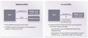
Even if error correction is present on the DRAM die, SoC designers may also implement error correction on the DRAM interface. In traditional designs that use DDR DRAM, such as servers and networking chips, error correction information is usually transmitted as a sideband to the DRAM data. However, when using LPDDR4 devices, the arrangement of LPDDR4 into 16bit channels, with two channels per die, two to four dies per package, and four channels per package, makes it impractical to use extra pins to transmit ECC. Instead, designers implement an in-line ECC scheme to transmit ECC data on the same pins as the data it protects (Figure 1).
Figure 1 Comparison of sideband vs in-line ECC strategies (Source: Synopsys)
Meeting automotive standards
SoCs designed to work in automotive contexts will have to meet automotive reliability standards such as AEC-Q100 and ISO 26262. DRAM interfaces on automotive SoCs will therefore also have to meet these standards, which can be achieved by using hardened IP developed for the purpose.
ISO 26262 has several requirements, including issues to do with processes, design and certification. One core requirement is to have a defined design safety methodology, and a safety manager to implement the resulting processes.
The DRAM interface IP itself has to have extra circuits to periodically test the interface to ensure that most errors that violate safety goals can be detected within a fraction of a second. Typically, a third-party certification is performed to rate the compliance of the design and assign an automotive safety integrity level (ASIL) rating. ASIL is a compound measure of safety, derived by combining the probability of exposure to a risk, its controllability by a driver, and the severity of the outcome if the risk causes a critical event. Most automotive designs need the DRAM interface to offer at least ASIL B protection of the DRAM interface: some designs may require the much more stringent ASIL D protection level, which is usually reserved for safety processors and their associated circuits.
Conclusion
DRAM will be much more widely used in automotive systems as displays, cameras, sensors and sophisticated ADAS functions become part of the vehicle’s safety-critical systems. With careful selection of discrete parts and interface IP, careful design and stringent processes, DRAM can provide the high-bandwidth and large-capacity storage necessary to enable these systems.
Further information
Synopsys provides a range of DDR interface IP including PHYs, controllers, verification IP, architecture design models, and prototyping systems.
Author
Marc Greenberg is the director of product marketing for DDR IP at Synopsys. He has 13 years of experience working with DDR Design IP and has held technical and product marketing positions at Denali and Cadence. He has a further 10 years of experience at Motorola in IP creation, IP management, and SoC methodology roles in Europe and the United States. He holds a five-year master’s degree in electronics from the University of Edinburgh in Scotland.

