FPGA-based prototyping to validate the integration of IP into an SoC
A case study describing validation of the integration of USB3.0 and USB2.0 interface IP that illustrates broader challenges FPGA-based prototyping presents.
This case study looks at some of the challenges and solutions you may face in integrating and validating USB interface IP within your SoC design and how to use FPGA-based prototyping to validate your system. It can be read in two ways
- As a source of useful guidelines on how to validate your internal projects as they encompass USB and other IPs typically supplied by third-parties;
- Or as an illustration of the role external design services play in developing FPGA-based prototypes for companies, allowing internal design teams to concentrate on core competences.
This specific project, addressing validation for USB 3.0/2.0 interface IP, was undertaken by Synopsys Professional Services.
FPGA-based prototyping
Several other good articles discuss the growing importance of FPGA-based prototyping including this Tech Design Forum guide, and also this extract from a jointly authored Synopsys/Xilinx technical manual.
Briefly, then, various prototyping techniques are seeing greater use because of a combination of time-to-market pressures and the increasing risk of re-spins posed during system validation.
The most frequently cited issue is the growing proportion of software in any major design project, making it vital that companies provide platforms on which software developers can begin work as early as possible. Preferably, this should be far in advance of first silicon so that it doesn’t become a project bottleneck.
IP proliferation also complicates integration. For example, standards families like MIPI are refined quite frequently and are becoming increasingly more complex. As the relevant interface IPs often come from third parties – developing internal ones is typically too lengthy and too costly – these present further challenges, especially when integrating within your system and validating that everything works together.
Virtual prototypes allow some software development work to begin while hardware is still at the system level. FPGA-based prototypes have typically come into use later. They are derived from near-final RTL, often for internal in-the-field system test and for supply to key customers so that they can also get a head start. However, hybrid techniques are bringing these techniques together to reduce delivery times still further.
Whichever mix of techniques your project requires (and both simulation and emulation will likely feature too), linear development is no longer an option.
Interface IP challenges
This study discusses USB 3.0/2.0 interface IP, but some general points are worth making first.
You can often run internal IP at slower speeds to accommodate the gap between the target performance of your ASIC and that of the FPGA for your prototype. However, external interfaces often have to run at higher clock rates required by their individual specifications.
More generally, an ASIC design will frequently have complex internal clock multiplexing that must be modified to allow for the more limited clocking resources and flexibility of an FPGA.
These factors alone show that you need a clear understanding of both prototyping techniques and the IPs to be integrated if you are to deploy the right methodologies and collateral – or you can engage a third party to do that for you.
At Synopsys Professional Services, we combine our own design expertise and experience with the wider company’s tools, DesignWare IPs and the HAPS family of FPGA-based prototyping hardware to fill that third-party role.
The prototype
Our target was to validate the integration of third-party supplied USB 3.0 IP into an SoC using the HAPS FPGA-based prototyping system.
A generic system for this task would comprise the following:
- One or more processor cores
- An interconnect fabric
- Third-party interface IP
- Custom design logic
Figure 1 provides a more detailed visual overview of the system we actually built.
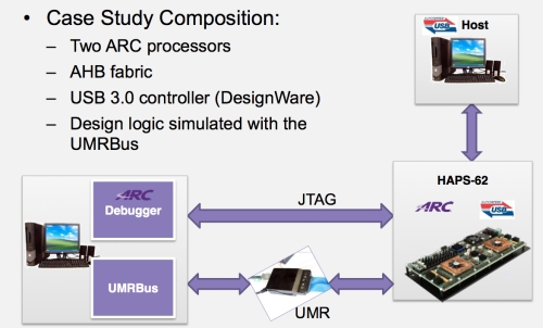
Figure 1. Case study design overview (Source: Synopsys)
As shown, the prototype was based around a Xilinx-based HAPS-62 board and consisted of two ARC processors. The latest HAPS-70 series allows for much higher capacity validation.
One processor carried out system level processing, including that for the USB controller. The other performed specific DSP functions and control for the third-party design.
The processors were attached to an AHB fabric. Each had its own instruction and data memory, and there was additional shared memory that both processors could access. The system also had a DMA controller attached to the AHB bus.
The USB controller is similarly attached to the AHB bus. A Synopsys USB PHY daughter card was used for the physical layer.
In addition to JTAG, a UMRBus was adopted as a convenient way of simulating data coming from and going to third-party IP. The UMRBus provides native data streaming from the host and is also particularly well suited to co-simulation with VCS and the implementation of custom interfaces to the host.
Alongside, HAPS, VCS and the UMRBus, here is a quick review of other Synopsys tools used for the prototype.
- Certify is an automated ASIC code conversion and partitioning suite to partition your ASIC design across many large FPGAs. It has tight integration with HAPS and DesignWare IP support to avoid ASIC-to-prototype mismatches.
- Synplify Premier provides FPGA synthesis and also has support for Synopsys DesignWare IP support to eliminate mismatches.
- Identify provides at-speed debug visibility at the RTL source and an almost unlimited number of debug signals and trigger conditions.
Assembling the prototype
There are several simple series of steps to follow in creating a prototype. Figure 2 provides a graphical overview.
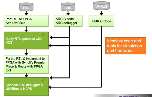
Figure 2. Design flow to modify and test FPGA-based prototype (Source: Synopsys)
The ASIC RTL is modified to make the design FPGA-friendly. Synplify will take care of a number of items automatically, such as clock gating conversion. But there will usually be a need for some specific modifications. For example, design changes that were specific to this prototype needed to be integrated, most notably the UMRBus interface.
Processor code will sometimes need to be developed. This was again true here as we needed to generate ARC code for the USB software driver. Test can also use ARC code that was used in simulation. With minimal or perhaps no modification, these tests can be rerun in the prototype for hardware validation.
UMRBus code was created, compiled and run in the simulation environment. This code uses simple APIs that can be called through C or C++. Alternatively, a TCL script can be used to interface to the UMRBus.
After these steps, we moved on to validating with VCS. We used both existing ASIC simulation tests and any tests and software that had been developed subsequently.
Then we implemented the RTL using Synplify. The project file can be built from the ASIC manifest file and any additional files that must be added for your prototype.
A further aspect of the implementation process was our use of the HAPSmap. This utility is provided by Synopsys to designate I/O pins such as the USB daughter card to the HapsTrak connectors. HAPSmap also provides an easy way to move the daughter card if you should need to add other HapsTrak connectors without having to reenter FPGA pin locations.
Once this implementation is done, the design is loaded into the HAPS motherboard.
The ARC debugger was connected to JTAG (the same debugger was used in simulation). The UMRBus interface was also the same as that designed and tested in simulation. These carry-overs eased the transition from simulation to the FPGA-based environment.
Then, we addressed the three sets of interfaces: USB, JTAG and the UMRBus. The USB set was the most important.
USB
There were two separate interfaces: one for USB 3.0, known as the pipe interface; and one for USB 2.0, with the ULPI interface being used in this project.
Pipe interface
A simple diagram of the USB 3.0 pipe interface is shown in Figure 3.
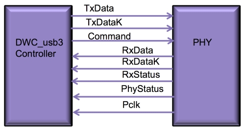
FIGURE 3. USB 3.0 Pipe Interface
ULPI interface
Achieving reliable performance required good control over I/O placement, the I/O registers and the clock skew.
The clock was 250MHz and the data width was 16bit. The interface was source synchronous with clock provided in both directions.
In addition, the PhyStatus signal required special attention, and our strategy is discussed further below.
A simple diagram of the USB ULPI interface is shown in Figure 4.
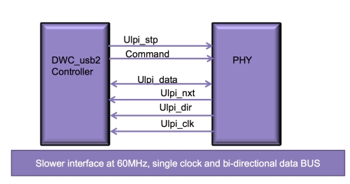
Figure 4. USB 2.0 ULPI interface
It runs at 60MHz. Instead of being source synchronous, it has a single clock and the data uses a bidirectional bus.
There are still possible clock skew issues. The clock internal to the FPGA must be skewed to sample the data correctly, and for the data sent by the FPGA to be sampled correctly on the PHY.
After reset, if the USB 2.0 PHY does not receive a command from the USB controller, the PHY will ‘hibernate’ and turn off the clock. It is important that the clock is appropriately aligned coming out of reset.
PHY challenges
As noted, the PhyStatus signal needs careful handling. It is used in the controller as both a clock and as data. We needed to meet set-up and hold time here at this register. We also needed to maintain PhyStatus in the same coherent timeframe as RxStatus.
As shown in Figure 5, one issue was that the tool placed ‘BUFG’ between PhyStatus and the clock and the input. This caused a long delay that resulted in transitions in PhyStatus taking place once cycle later than other pipe data inputs.
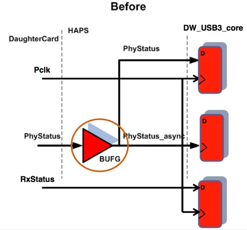
Figure 5. PHY challenges – before (Source: Synopsys)
Specifically, RxStatus did not suffer from this latency, and this impacted receiver detection. Here, the controller is looking for PhyStatus to become active at the same time that RxStatus is set to 3. This is the PHY telling the controller that there is a receiver connected to the end of the USB bus.
If there is a large latency and this process is pushed off to the next clock cycle while RxStatus is at 0, the controller will see no receiver. It will make several attempts to find one, but will eventually time out and stop. This obviously will also stop the training sequence.
Our solution is shown in Figure 6. We manually shifted ‘BUFG‘ so that while it still drives the clock inputs, PhyStatus is now going to the input in the register with the same latency, and set up and hold time as RxStatus. So, the controller sees the outputs with PhyStatus going high and RxStatus at 3, complete receiver detection and moving on to poll a full training sequence.
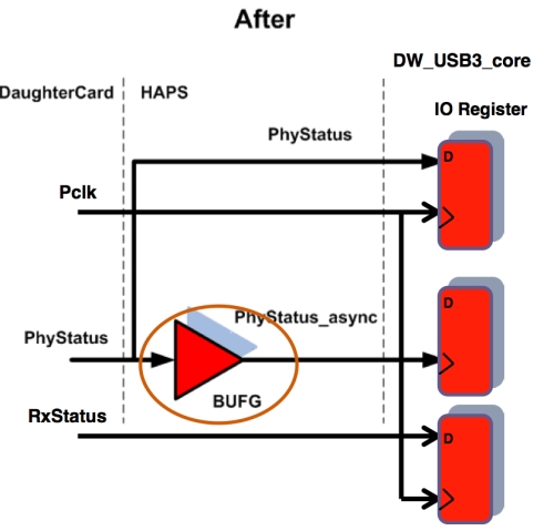
Figure 6. PHY challenges – after (Source: Synopsys)
Clocking challenges
The USB controller multiplexes clocks between USB 3.0, USB 2.0 and sleep modes using global clock buffers. This complicated structure gave us cascaded clock buffers and could have led a large insertion delay difference between the different domains.
Our concerns here can be seen by tracing the ‘raw’ ULPI’ clock in Figure 7. However, the graphic also shows the solution. We were able to use the ‘fast track’ feature provided by the Xilinx Virtex-6 FPGA to minimize hold time.
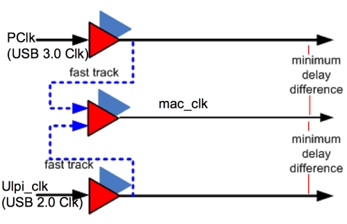
Figure 7. Addressing clocking challenges (Source: Synopsys)
‘Fast track’ gives you a high speed path to a clock buffer as long as you use adjacent global buffers next to your multiplexer. This minimized worries about turnaround time and hold.
We then needed to consider the interface clocking.
The USB 3.0 pipe interface required the use of Xilinx I/O registers to determine the correct setup and hold times. The clock skew had to be adjusted to be at the center of the data eye.
The prototype used the Xilinx multimode clock module (MMCM) to set this skew. It works in essentially the same way for USB 3.0 and USB 2.0. The clock comes in, goes through the MMCM and is phase adjusted, as shown in Figure 8. This phase adjustment will be such that the clocks centers within the sample of the data coming in.
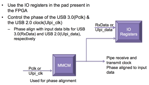
Figure 8. Meeting setup/hold time (Source: Synopsys)
The adjustment was carried out with the help of Identify. In the tool, we instrumented PhyStatus and the RxStatus for USB 3.0 and then shifted the clock earlier in time (or to the left) until we saw a failure. Then we shifted it later (to the right) first to where it would start working and then to where it failed. The center of that shift indicated where the data eye was.
We were able to do this using a script that changed the phase delay through the MMCM without have to go through place and route. Turnaround time was just a few minutes.
The USB 2.0 clock was less critical. It runs at a much slower speed. This we could move in 45-degree increments until it worked. Once it was set, we did not have to reset it.
Timing challenges
A USB controller will be designed for optimum performance in the final ASIC. Therefore, there should not be issues with meeting timing requirements. But an FPGA does not have the same level of performance.
To resolve this, Synplify Premier’s place and route chain can produce bit files that will work under laboratory conditions for your prototype. The trick is determining the right ones. We found that the best way to do that within the shortest turnaround time was to perform many P&R runs in parallel with different switches to find the combination that yields the most comparable performance.
We then reviewed the best timing results, picked the ones with the least negative slack and tested those in the lab for operation.
Debug
This section goes deeper into how we used Identify. We have already seen how it was used to discover PhyStatus and set the proper clock skew.
Identify allowed tracing of event states up to the link, so we could detect when we came out of receiver detection or went into polling. The ability to trace the interface, the link states and the substate events was critical in bringing up the prototype.
The RTL Instrumentor used with the Identify Instrumentor allowed the team to browse RTL code under test and pick signals to instrument in much the same way as they would in a simulator environment with DVE. A designer could see exactly what he wanted to capture.
Identify also provided area estimation so that we could make tradeoffs between the amount of instrumentation versus the FPGA area consumed. This process was automated with TCL scripts, and the ease of use greatly sped up debugging of the case study prototype.
All these features increased both efficiency and accuracy in determining what signals to instrument.
As shown in Figure 9, the Identify Debugger also offered a familiar environment to that for simulation. Visibility was provided to browse signals and set triggers.
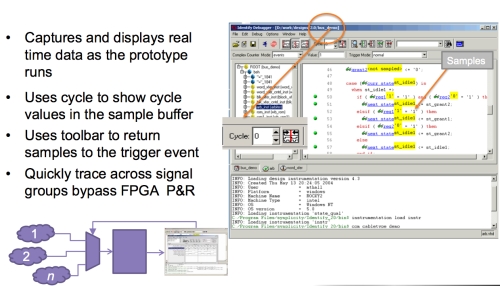
Figure 9. Identify Debugger for simulator-like signal browsing (Source: Synopsys)
Values were annotated to the source code just as they are in DVE. We could move through the process cycle by cycle and watch the values change in the source code in order to debug the RTL. Signal groups could be traced, bypassing the impact of signal changes that can occur as a result of FPGA place and route.
Figure 9. USB interface debugging with Identify
UMRbus and JTAG
With regard to the two remaining interfaces, we can briefly note for now that JTAG was used by the ARC debugger.
The UMRBus interface can be designed for unique design requirements or VCS co-simulation. In our project, it provided a high-speed link between the host and the HAPS prototype, over a 32-bit rather than an 8-bit interface using HapsTrak.
An 8-bit interface was available over the CDE connection. The bit file could be downloaded through the CDE in this design to speed up FPGA configurations.
The connection from the host to the UMRBus was made over a four-lane PCIe cable.
Hardware verification
The hardware needed to be verified before it could be delivered to a software team. Sometimes, as was the case here, this was also before there was specific system software available.
We therefore needed to create a simple USB driver that could function without an operating system. This was done on a host PC, based on WINUSB. The driver allowed us to send millions of packets to the USB subsystem, testing the data integrity and USB performance of the prototype.
The software team received a prototype that was tested and a simple software driver to leverage for their own development.
Once the test software was developed, we used the ARC MetaWare debugger to test and integrate it into the prototype. The ARC debugger uses JTAG to provide a GUI-based debug environment built around the popular Eclipse interface.
The same debugger can be used with the VCS simulator to make a seamless transition from simulation to hardware debug. Break points, watch points and all common emulation tasks can be performed in this GUI interface.
The ARC debugger also offers multiprocessor control. This is also a very similar GUI to what you may be used to in other processors.
Conclusions
This case study highlights many of the complex challenges presented in completing FPGA-based prototype in the most efficient way.
An integrated solution that uses a comprehensive set of tools and services to get an FPGA-based prototype up and running quickly certainly helps. It enables easier translation across different techniques such as prototyping, simulation and emulation.
Additionally, experts in not only the various types of IP themselves, but also how to integrate and validate IP in a system are available. They can help alleviate much of the pain. Synopsys Professional Services offers that breadth of knowledge and expertise across various designs, including though not limited to comprehensive experience with DesignWare IP and FPGA-based prototyping hardware and software tools.
About the author
John Kuhns is a senior design consultant at Synopsys Professional Services with 13 years of experience, specializing in FPGA prototyping. Before joining SPS, he was with Lockheed Martin for 23 years.
