Fast, accurate layout merging for SoC flows
How to achieve efficient merging of data from formats such as OASIS, GDS, and OpenAccess to ensure timely verification through DRC runs.
System-on-chip (SoC) design teams typically run full-chip design rule checking (DRC) verification multiple times throughout the design implementation. This best practice lets design teams find any chip-level violations between block instances early in the design flow, when they are easier to correct. However, assembling the latest physical layout data for each block and merging it into a single OASIS or GDSII database for full-chip verification can be difficult and time-consuming. To perform these DRC runs with the needed frequency, chip-level designers need a fast, reliable data merging flow that satisfies the needs of the continuous-build parallel design implementation flow while minimizing or eliminating time-intensive data management activities.
Database format conversion
One of the first issues that must be resolved is database conversion. A full-chip database always uses either the GDS or the OASIS format. External or intellectual property (IP) blocks already in the OASIS/GDS format can simply be referenced for merger during layout export from the place and route (P&R) tool as chip-level OASIS or GDS files. However, if some external block data is not available in the OASIS/GDS format, chip-level export and full-chip verification cannot happen until these data sources have been converted.
Intermediate database formats
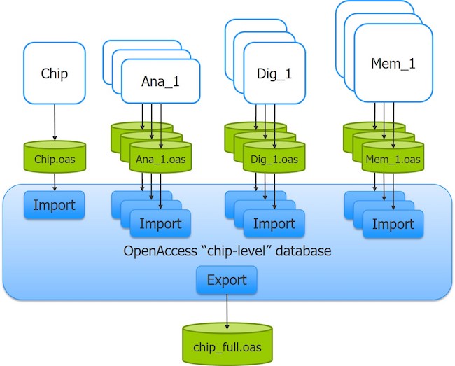
Internal data merging flows that use intermediate databases like OpenAccess can create unintended bottlenecks. These flows require that all the blocks and the chip-level design are converted to and stored in the OpenAccess format. This final OpenAccess chip-level database design is then exported to GDS or OASIS (Figure 1). As the blocks and chip-level design are exported to the GDS/OASIS chip-level database and merged, chip-level block abstracts are replaced with the physical design blocks, and this creates a full hierarchical database. Unfortunately, runtime requirements for this multiple translation flow make its use prohibitive. Some users report data merging under it taking up to 20 hours to finish for a full chip.

Figure 1. Intermediate ‘chip-level’ databases require multiple data translations and incur significant time penalties (Mentor)
Unless the use of intermediate database formats is unavoidable, it should be discouraged during physical verification iterations. If you minimizing or eliminating the use of intermediate conversions, design teams gain more time to analyze results and fix layouts within delivery schedules.
Database updates
All the data being merged should be the latest version of that data. If any chip-level data is exported with an out-of-date reference, the output violations for the DRC run will be invalid. The chip-level team will have to re-run both the data export and merger, delaying delivery.
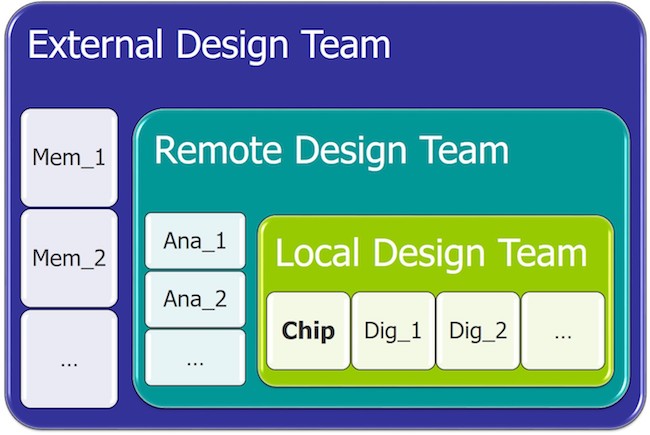
However, ensuring that all data is up-to-date is not always straightforward. Block development is often done in parallel with chip-level implementation, meaning the work is distributed between internal and external teams. For any SoC, there may be dozens of designs in various stages of development at a single time. In addition, block development teams working in parallel may be located at different internal sites, and/or in different time zones. Even co-located teams may have different work schedules. Some blocks may be assigned to an external team or contractor who may not have internal network access, and that could delay data transfer (Figure 2). Being aware of and accounting for any or all of these concerns when planning the data merge flow helps ensure all data is current for each interim chip-level DRC run.

Figure 2. Ensuring physical layout data is up-to-date before full-chip DRC can be difficult when you have to coordinate with multiple design teams (Mentor)
Defining a schedule for full-chip data merge and physical verification runs is one technique that can help mitigate these issues. If all teams and suppliers are aware of the schedule for full-chip verification runs, they can ensure their block data is up-to-date and available in the required format when needed.
Database merging
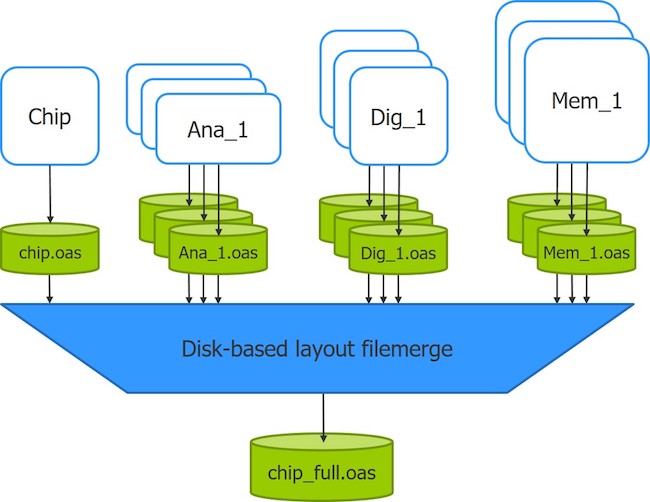
Once you know you have up-to-date data, the next step is to manage the data merger. Many database filemerge utilities must read each database into memory before merging them in a single full-chip database. This approach not only requires a significant amount of system memory. It also results in extensive runtimes when used with full-chip verification flows. Using a disk-based in-memory merging utility (layout merge) lets you merge multiple input OASIS or GDS databases into a complete hierarchical database for full-chip DRC without having to read each database into memory first (Figure 3). This technique dramatically reduces memory requirements and enables faster runtimes than in-memory merging solutions.

Figure 3. A disk-based layout filemerge quickly merges multiple blocks and chip-level data to create a full-chip database (Mentor)
File merging processes typically have three merge modes: overwrite, append, and rename. Overwriting the chip-level abstract placements with the physical layout data in the individual block OASIS inputs is usually the default mode for a layout filemerge process. Updated static layout files from the block teams are used to overwrite any corresponding blocks in the chip-level design file before export to the GDS/OASIS database.
Individual block updates
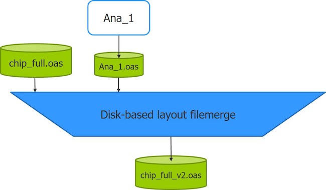
Sometimes, after the full-chip file merge is complete, a design team working in a continuous build environment finds errors in a block that require correction before running the chip-level DRC iteration. With a disk-based in-memory layout filemerge flow, individual blocks can easily be updated without requiring the re-export of any data that did not need modification (Figure 4).

Figure 4. The block Ana_1.oas has been updated and replaced in a new version of the chip-level database (chip_ full_v2.oas), without requiring the re-merging of all of the inputs in the original chip-level database (chip_full.oas) (Mentor)
OASIS data compression
The OASIS format has several features that help reduce file size compared to the GDS format [1].
- OASIS data represents numerical values with variable byte lengths, whereas the GDS uses fixed byte lengths.
- OASIS functionality can recognize complex patterns within a layout and store them as repetitions, rather than as individual instances or geometry objects.
- The OASIS CBLOCKs feature applies Gzip compression to the individual cells within a layout. Because this compression is internal to the file, tools do not need to create a temporary uncompressed file, as is often necessary with normal Gzip compression. Additionally, unzipping a Gzip file is typically a single-threaded process, whereas CBLOCKs can be uncompressed in parallel.
- STRICT mode OASIS layouts contain an internal lookup table that can tell a reader the location of different cells within a file. This information allows the reader to more efficiently parallelize the loading of the layout and can offer significant loading time improvement.
When the output format is OASIS, CBLOCK compression can further compress OASIS files, while STRICT mode shortens read time for downstream tools. Although features such as CBLOCK compression and STRICT mode are not required, we highly recommended that layout designers use both to realize the fastest loading times while maintaining small file sizes.
Conclusion
Running multiple intermediate full-chip DRC verifications on an SoC during parallel implementation lets designers find and fix errors earlier in the design flow, minimizing the risk of late design changes that can delay tapeout. However, efficient data updating and merging processes are needed to ensure these verification runs can be performed in a timely manner and deliver accurate results. A fast, comprehensive disk-based in-memory merging solution delivers excellent runtime performance with low memory utilization.
References
[1] Dennis Joseph. “Stop waiting for GDS layouts to finish loading—It’s time to switch to the OASIS format,” Mentor, a Siemens Business. April 2018.
About the author
James Paris is a Technical Marketing Engineer with the Design to Silicon Division of Mentor, a Siemens Business, supporting Calibre design interfaces. Prior to joining Mentor, he was responsible for analog/mixed-signal physical design implementation and flow development for various IC design companies. James holds a B.S. in Computer-Aided Design Engineering and an M.B.A in Marketing. He can be reached at jamesUNDERSCOREparisATmentor.com