Device native debug and verification for FPGA
GateRocket’s RocketDrive facilitates integration of an FPGA into an HDL simulator to provide a “native” execution of a design on its target FPGA device. The companion RocketVision tool provides software-debugging capabilities that directly identify and enable the rapid resolution of bugs. This article considers the use of these tools in a “device native” verification and debug methodology, with specific reference to a communications design undertaken by Empirix, a specialist in voice applications test and monitoring.
The long loop
There is an unstated impression in FPGA design that the process of capturing a design, translating it into a configuration file, and loading that configuration into the silicon consumes relatively little time and effort.
That may have been true 10 years ago when FPGAs contained the equivalent of only a few thousand logic gates. Today’s state-of-the-art devices can contain not only millions of logic gates, but also thousands of DSP functions, megabits of RAM, and a multitude of other hard IP core functions (Figure 1). This causes major problems with regard to verifying the functionality of the design, because a software simulation run of the full-chip RTL that was once completed in hours can now take days or weeks. In turn, designers are often forced to move their FPGA quickly to the system lab where tests run at system speed, but here, a lack of visibility and controllability make debugging an arduous task.
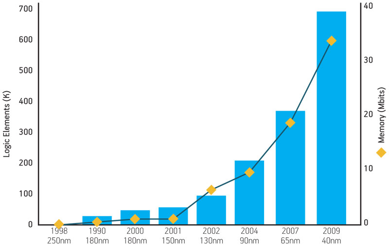
Figure 1
The rapid increase in FPGA complexity
The result is a ‘long loop’ when it comes to detecting, isolating, debugging and fixing any bugs. In many cases, actually identifying the source of a bug can be problematic, because logic, intellectual property, timing and tool flow errors are all mixed together and hard to distinguish. Furthermore, the only visibility into the FPGA is via on-chip logic analyzers that are limited in terms of the number of signals they can observe and the depth of memory to store signal history. Then, once a bug has been identified, the process of making a change and rebuilding a complex FPGA can take a day or longer. It is easy to see how this slow, iterative process can become unwieldy, and can lead to weeks or months of project delays.
A recent survey by FPGA Journal found that the process for identifying and fixing FPGAs by looping from the lab where a bug is identified, back through simulation, synthesis, and place and route (P&R) adds between 92 and 148 days to the design process.
Empirix
Empirix is a leading provider of voice application testing and monitoring solutions. Its Hammer XMS products are used to test the performance, capacity and quality of voice and multimedia networks using such standards as voice over Internet Protocol (VoIP), Next Generation Networks (NGN) and IP Multimedia Subsystems (IMS). The majority of the world’s leading network equipment manufacturers, service providers and Fortune 100 companies depend on Empirix products to help them adopt these technologies with confidence.
At the heart of many Empirix solutions is an advanced FPGA that must emulate and detect complex network protocols and long serialized messages. As the Empirix engineering team embarked on a next-generation platform design, it recalled lessons learned from its previous FPGA-based project.
On that FPGA design they simulated the equivalent of about 100ms of real-time activity to verify all the basic functionality of the device, and then moved to the lab to complete the validation and debug the design in a system environment. What they expected would take weeks ended up taking months.
First, they had to trade off FPGA resources between product functionality and on-chip logic analyzer signal capture/storage. Second, given the finite amount of on-chip block RAM, they had to sacrifice the breadth of signals that could be observed in order to get adequate depth for capture memories to store the results of long runs. That led to multiple painful iterations.
- They would trace back a particular failure only to discover that there was a critical signal missing. In order to add access to that signal, the team had to re-compile and re-map the design, a process that could take between 12 and 15 hours.
- It was also difficult to distinguish between logic errors, timing issues and intellectual property- or tool flow-related bugs. All these problems were mixed together at the system level. That made finding the root cause of any problem tougher still.
The bottom line is that debugging FPGAs in the system is like looking at a complex world through a keyhole—you get a very narrow view, and it often does not include what you actually need to see.
Next-generation design
Empirix’s subsequent FPGA project was even more complex and relied on a new silicon family as well as new, complex intellectual property blocks. The FPGA design consumed 74% of the chip’s logic resources and 100% of the block-RAM, leaving no extra memory for on-chip logic analyzers. The team agreed that it needed much more powerful verification and debugging tools in order to manage the complexity of the design, and avoid a protracted debugging period that could delay the product’s introduction.
Consequently, Empirix decided to purchase the RocketDrive system and RocketVision from GateRocket. They selected RocketDrive with the aim that it would extend their existing simulation environment in a way that enabled the detection of bugs in simulation that would otherwise slip through to system integration. The companion product, RocketVision, was then intended to give them access to the internal signals of the native FPGA hardware from their simulation debug environment, automatically detecting any mismatches between the simulation model and the actual silicon.
GateRocket combines actual FPGA hardware and RTL simulation models in the same verification run (Figure 2, p. 41). The RocketDrive is available in the form of a removable caddy (Figure 3) that plugs into a standard 5¼” drive bay on a deskside workstation. RocketDrives come in a variety of models, each targeted toward a different family of FPGAs from Altera or Xilinx. In each case, the RocketDrive contains the largest member of the family with which you are working.
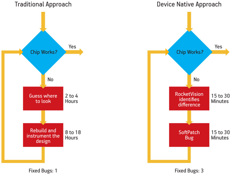
Figure 2
Traditional and ‘device native’ flows
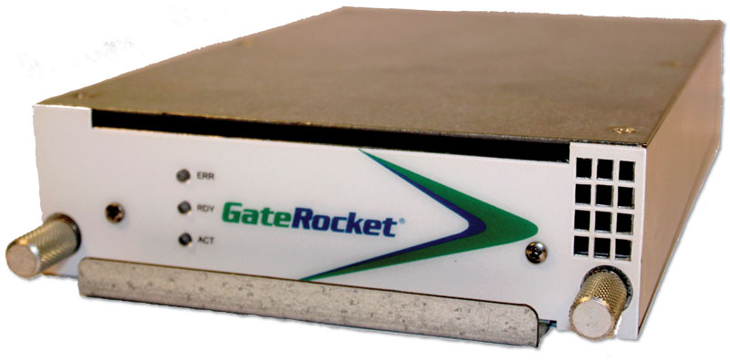
Figure 3
RocketDrive
Empirix used the RocketDrive on its next-generation project for full chip, silicon-accurate verification after RTL simulation had been completed and prior to system-level integration in the lab. It helped the team discover a number of bugs, including errors in the declaration of certain inputs and outputs to the logic synthesis tool. In themselves, these were relatively simple errors, but they would have taken weeks to debug in the lab environment. They were apparent in the RocketDrive because it validates the behavior of the actual FPGA hardware after synthesis and P&R.
Reuse
The RocketDrive has also been designed for use on projects where there are previously proven functional blocks. Using RocketVision, engineers can direct the system to place all of the previously proven blocks in the RocketDrive, and to keep any unverified third-party IP blocks and any new blocks developed in the software simulator. This immediately allows faster simulation iterations.
As each new block is verified at the RTL (or behavioral) level in the context of the full-chip design, its synthesized, gate-level equivalent can be moved over into the physical FPGA in the RocketDrive. As soon as a problem manifests itself, the verification run can be repeated with the RTL version of the suspect block resident in the simulation world running in parallel with the gate-level version realized in the physical FPGA. By means of RocketVision, the signals from the peripheries of these blocks (along with any designated signals internal to the blocks) can be compared on the fly.
Benefits of ‘device native’ verification
Using the combination of conventional simulation with physical hardware and an appropriate debugging environment, engineers can very quickly detect, isolate and identify bugs, irrespective of where they might originate in the FPGA design flow. Once a bug has been isolated in one block of the design, a change can be made to the RTL representation of that block, which can then be re-run along with the hardware representation of the other blocks. In this way, a fix can be immediately tested and verified without re-running synthesis and P&R, and with only the suspect block running in the software simulator.
In the context of the above-mentioned survey’s results, GateRocket can reduce the ‘long loop’ process by 55% as it allows the same bugs to be found and fixed during the simulation phase. By getting the simulator to perform like a development board, designers are encouraged to undertake more debugging at that stage, saving time in the lab later on.
Empirix says that its experience bore out this claim. “If an FPGA design runs in the RocketDrive then we are confident that it will run in the system. That saves us weeks of system debugging time and dozens of RTL-to-bitstream iterations, each of which takes us two days or more,” says engineering manager Mike Garofolo “Overall, the RocketDrive has saved us at least two man-months on the very first project, and we expect that it will have even more value in the future as we exploit more of its capabilities for both block and chip-level verification.
“The bottom line is that GateRocket significantly reduces the risk of complex FPGA development and gives my team a lot more confidence in the schedule than they’ve had in past projects. And in the competitive market we’re in, that’s priceless.”
Dave Orecchio, is president and CEO of GateRocket, has 24 years of semiconductor industry experience at four venture capital-backed companies with a focus on semiconductors, ASIC and FPGA design and development. He has held executive positions in marketing, sales and general management at LTX, Viewlogic Systems, Synopsys, Innoveda, Parametric Technologies and DAFCA.
GateRocket Inc.
19 Crosby Drive
Suite 100
Bedford
MA 01730
USA
T: +1 781 908 0082
W: www.gaterocket.com