Confronting chip assembly challenges
Until recently, hierarchical design flows have been favored for the implementation of multi-million gate SOCs. However the rapid increases in design size brought on by nanometer process geometries have seen engineers seek to cope with the inherently block-based nature of such flows by seeking greater concurrency between the block implementation and chip assembly stages in the hierarchical structure.
Here, designers have faced limitations largely created by the tools available to them. The article identifies five areas in particular – abstraction-generated violations, bad budgets, bad pin assignments/block placements, clock tree synthesis limitations, and full-chip static timing analysis limitations – that lead to problems only becoming apparent late in a design project’s life, with serious implications for factors such as a successful design to specification and time-to-market.
In response, the article proposes a methodology based on a new generation of tools that addresses four aspects of chip assembly and associated flow steps – infrastructure enhancements, full-chip static timing analysis engines, chip closure optimization and chip-level clock tree synthesis – and puts more power to deal with variability and other factors into the hands of the designer.
At nanometer process nodes, physical design teams are producing multi-million gate SoCs with very complex functionality that draws on the integration of elements such as different processor cores, memory blocks, soft and hard intellectual property (IP) blocks, and analog circuitry on a single chip. In addition to size and complexity, engineers must also deal with variations in design modes, environmental conditions, design-for-manufacturing issues, and device/interconnect behavior.
In recent years, hierarchical design flows have gained traction for the implementation of multi-million gate SOCs. However as design size increases, flows that use the current generation of physical implementation tools are coming under severe strain to deliver chips to specification on aggressive schedules.
Engineers have historically used hierarchical methodologies (breaking the design into pieces or blocks) to extend the capacity of EDA tools, improve tool run-times, and hedge against last minute design changes. A hierarchical flow typically includes:
- Chip planning (design partitioning, time budgeting, block placement, pin assignment, power and clock planning);
- Block implementation (placement, clock tree synthesis (CTS), optimization, routing);
- Chip assembly (block instantiation, top-level glue logic optimization, top-level CTS/routing, global wire buffering, power and clock routing, etc.).
Chip planning is done early in the design flow and is a ‘guestimate’ based on the available design information. Chip assembly is the last step in the implementation phase when all the blocks are reassembled after detailed block-level implementations. Any wrong decisions or assumptions made during chip planning and block implementation are exposed at this stage, and they will lead to further, sometimes unnecessary design iterations and missed delivery dates.
Because of the risks posed by surprises occuring late in the project flow, designers have been strenuously seeking to achieve concurrent engineering of the block implementation and chip assembly steps. This article reviews the chip assembly challenges and discusses the requirements for a strategy that comprehensively addresses all the issues those challenges present.
Chip assembly challenges
In order to better understand the chip assembly challenges, let us look at a recent design project that encountered many of them. The specifications were: 21 million gates in six partitions, 90nm, 300MHz, 500+ RAMs, three functional and two test modes, and five timing corners with OCV modeling. The design was partitioned into six blocks and a detailed implementation completed for each block separately. The design team then had to assemble the full chip in order to verify chip-level performance. Some of the rude surprises that awaited them at the chip-level included:
- Abstraction-generated violations;
- Bad budgets;
- Bad pin assignments/block placements
- Clock tree synthesis limitations;
- Full-chip static timing analysis (STA) limitations.
Let’s consider each of these areas in turn.
Abstraction-generated violations
In order to work around the capacity limitations of current physical design tools, the team had to abstract the timing and the physical views of the six blocks. Unfortunately, after fixing some timing violations with the abstracted flow, they still encountered others on paths that spanned across blocks.
Abstraction inherently results in a loss of accuracy. The sources of this loss range from black-box models to interface logic models. In most cases, these models are ‘read-only’ and this severely limits the amount of optimization that can be done at the top-level. Even when models are ‘writable’, designers must dedicate a significant effort to keeping the models in-sync with the original data. This adds to the complexity of achieving the desired full-chip performance and can cause major delays.
The only reason for abstraction is the inherent capacity limitations of current-generation IC implementation tools and the lack of a flexible infrastructure that supports true hierarchical design. A system with large capacity that gives users the option to adopt different levels of abstraction for different blocks can help alleviate this loss of accuracy.
It should also be noted that, at 90nm and below, problems with accuracy are amplified when designers have to optimize their work for multiple modes and corners. A separate abstraction model must be created for each scenario.Moreover, no current modeling technique accounts for signal integrity effects within the terms of the abstraction.
Bad Budgets
The designers in our case study did not have accurate predictions of top-level global path timing and inter-block routing during chip planning. As a result some of the block budgets were practically unachievable. The resulting poor boundary timing constraints created a problem because the timing of block I/O paths could not be changed significantly during top-level design optimization due to the presence of abstract models.
In general, it is difficult to set a good I/O budget for every block in a hierarchical design and this can lead to problems during chip assembly. Design teams have tried to address this issue with architectural changes such as register-bounded physical blocks. However, such changes impose too many artificial restrictions at the architecture level (e.g., extra pipeline stages) to address what is fundamentally a physical design tool limitation.
Bad pin assignments/block placement
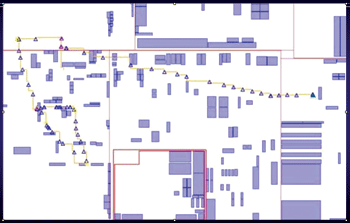
Figure 1. Bad block budgets due to inaccurate prediction of global paths
Pin assignment is today a process that is fairly decoupled from timing closure at the full chip level. A chip-level path may fail its timing constraints because of sub-optimal pin assignments as it goes from one block to the next. However, the feedback loop for pin assignment is today driven by routing only, and there is no consideration of the need to keep pins that correspond to timingcritical paths close to each other, nor of the need to spread out pins that belong to positive slack paths. Pin assignment cannot be cast in stone and needs to revisited at the full-chip level in order to achieve maximum flexibility and thus close top-level timing.
CTS limitations
Full-chip clock assembly is one of the most difficult design tasks. It requires engineers to predict insertion delay targets for the blocks and balance the lower-level clock trees at the top-level, while also considering effects such as on-chip variation and operation over different modes. Predicting those targets is very complicated, and can even prove impossible, where the design includes inter-block and feedback paths.
More often that not, design teams resort to manual editing of the top-level clock tree in order to achieve skew and latency targets. The option of doing a full-chip, top-down CTS that balances the overall chip-clocks is not available in today’s design flows because of capacity issues and the inability of CTS engines to deal natively with physical hierarchy issues.
Full-chip STA limitations
In this project, the chip-level timer lacked advanced capabilities that would have allowed it to address such issues as modes, corners, case analysis, and complex clocking. The designers were forced to iteratively analyze and optimize each scenario individually. The obvious issues that arise here were exacerbated by the fact that there were a lot of dirty constraints from the initial chip assembly. The lack of a variability-aware incremental analysis infrastructure that enabled rapid ‘what-if ’ queries for comprehensive analysis resulted in long run times and wasted effort. A wider point here is that no timer in the market today has been designed to comprehensively address such variability concerns. Also, the sheer size of a design by the chip assembly stage renders the current-generation of implementation systems ineffecient when they are benchmarked against their ability to analyze a design accurately in a reasonable run-time.
The solution
Several challenges have to be addressed if we are to architect a physical design system that addresses all the aspects of chip assembly and design variability highlighted above. Some of the most fundamental of these are the needs for:
- Infrastructure enhancements;
- A full-chip STA engine;
- Chip closure optimization;
- Chip-level CTS.
Again, let’s consider each of these in turn.
Infrastructure Enhancements
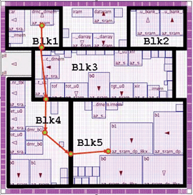
Figure 2. Full-chip timing analysis for inter block paths
Abstraction should be not be a requirement for chip assembly. The user should be given the freedom to choose which blocks to abstract and which not to abstract, depending upon the top-level paths and the level of accuracy needed. For example, a block that is cloned heavily may be abstracted while a block that is not cloned need not be abstracted either. Such flexibility will bring greater accuracy to chip-level timing measurements.
Ideally – and if feasible – designers want a ‘flat’ view of the entire chip for accurate analysis and optimization while fully preserving the block-level design interfaces. To implement this, a high capacity data model is desirable, one that can represent arbitrary levels of logical and physical hierarchy. The data model must also be able to
efficiently represent all the physical information for the blocks and the full-chip. Indeed, given the advent of 65nm design, the model should have the capacity to represent 50-80 million-gate designs with no abstractions whatsoever.
Full chip STA engine
In order to address nanometer effects, the timing engine should seamlessly handle modes/corners, complex clocking, case analysis and other sign-off timing features on the basis of compact memory usage and a fast run-time.
Chip assembly represents the ‘stress test’ for the capacity of the physical design and timing data models. It is important that the analysis infrastructure (extraction, delay calculation and STA) be incremental to enable rapid ‘what-if ’ queries.
In addition, capabilities like constraint debug and an ability to handle ‘dirty’ data are critical to ensure that chip assembly is performed concurrently during implementation. The expectation should be that a full-chip analysis of a 30 million-gate design – with extraction, delay calculation and STA – will take less than two hours.
Chip closure optimization
When users have sufficient flexibility in determining their preferred level of abstraction and access to a full-chip analysis engine that is both fast and accurate, we will be at a point where chip-level timing closure can be achieved efficiently.
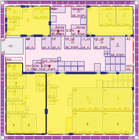
Figure 3. Flat view optimization with physical hierarchies
Optimization algorithms can then be given the freedom to work on both top-level and block-level logic to help deliver chip performance to specification. In addition, the optimization engines will be able to review pin assignment decisions incrementally and adjust them to obtain even better performance.
Since block-level boundaries are maintained at every stage of the flow, the changes made to the blocks at the chip assembly stage will directly update the block-level implementations. Steps such as detailed routing can still be done at the block-level for the sake of run-time. Full-chip performance can be optimized with minimum restrictions on the levels at which logic changes are applied.
Again the key here is flexibility. If designers choose to keep a certain block-level representation intact at top-level (due to cloning), they can then choose to mark those blocks that are not to be modified and let the optimization engine work on everything else. As with other elements, the optimization engine needs to be very efficient in memory and runtime to be able to operate at the 50-80 million-gate level without incurring significant run-time penalties.
Typically, multi-mode timing also plays a big role at this stage as the chip needs to be verified over all modes of operation. Having a native design for variability infrastructure, enables efficient and correct analysis and optimization at the full-chip level.
Given the ability to load the complete design without any abstractions and the ability to analyze multiple variations simultaneously, the next logical step is to optimize the design to meet all its variation constraints based on a flat view of the complete chip.
The tools here must view the design from a full-chip perspective to ensure better timing closure than can be achieved when designing different blocks in isolation. Such a design process involves adequate repeater placement along with matching interconnect and cell delays to meet setup-and-hold and clock-skew specifications. In addition, a hierarchical-design physical-implementation tool should minimize or eliminate top-level wiring channels. These can increase chip size by 20% or more over the area of a flat design.
The physical implementation tool must also be able to run reasonably fast, allowing the user to iterate and re-optimize as needed to meet design specifications. Pin reassignment to alleviate congestion issues, re-budgeting to correct wrong block budgets, and automatic push-down/pop-up technologies to manage physical and logical correspondence after optimization are all required to achieve the fastest design closure.
Chip level CTS
CTS represents one of the biggest challenges in chip assembly. With the proliferation of mobile devices, clock trees have become extremely complex circuits with different clock tracing per circuit mode of operation.
During chip assembly, the designer should have the flexibility of choosing either to build the clock tree top-down (with block-level interfaces preserved) for the complete chip, or to balance some or all lower-level clocks at the chip level. Bottom-up clock assembly requires that the CTS engine can understand the physical hierarchy and build the upstream trees given a set of block-level trees. Also at the chip level, issues such as clock balancing across multiple clock domains need to be addressed.
Unfortunately, the current state of the art in this area is mostly based on manual scripting to address these challenges on a case-bycase basis. One key observation that needs making is that accurate clock tracing during STA performs all the analysis needed for chip-level CTS construction. A CTS engine tightly integrated with a full-chip signoff STA engine can automatically detect these requirements and significantly reduce the manual effort required.
Also, current physical design flows restrict design teams to performing clock tree construction block-by-block due to capacity limitations. If the ability to provide fast full-chip clock tree construction were provided with full cognizance of block-level interfaces, it would yield a higher quality clock tree with fewer buffers. Here again, the decision as to the type of clock tree methodology has to be made by the design team based not on limitations in tool capacity, but rather on what is the most efficient way to get the best clock tree.What we need is a flexible clock tree infrastructure that enables either a full top-down or bottom-up approach – or some hybrid of the two.
Conclusion
Design teams are being adversely affected by the lack of chip assembly capabilities in addition to the phenomenon of variability in nanometer technologies. Abstractions, bad pin assignments, wrong block budgets, lack of variability-aware analysis engines, and a dearth of concurrent optimization capabilities often lead to chip failures, reduced yields, missed schedules and lost performance. A new paradigm and tool set that enables multi-million gate chip assembly while concurrently analyzing and optimizing over number of design variations is critical for hierarchical flows at 90nm and below.
Sierra Design Automation
Corporate Headquarters
3250 Jay Street
Santa Clara
CA 95054
USA
T: +1 408 986 8700
W: Sierra Design Automation was acquired by Mentor Graphics in 2007