Where tools end and best practices begin
Design tools can only do so much. However many functions they contain, checks they perform or disciplines within a project they address, they are only as good as the internal design strategies applied while using them.
A truism? Yes, it is. But given the increasing technological challenges all design teams face, it is one that can easily be forgotten. Because not only are those challenges growing in number; they are also becoming increasingly complex.
Mentor Graphics is the market leader for software in the printed circuit board market. Last month, we announced the winners in the 26th edition of our PCB Technology Leadership Awards.
Among the successful designs were efforts that pushed the limits in terms of layers (the highest we saw was 24), vias (55,000 was the record there), nets (as high as 7,000), connections (31,000), components (7,000) and FPGAs (20). The largest percentage of high-speed nets we saw in a single project was 90%.
Hitting numbers like those requires great skill, a willingness to extend engineering’s boundaries and, we are happy to note, an efficient use of Mentor tools.
But equally – if not more – important is the fact that delivering a board on time, within a very complex and tight specification, and within the likely context of multiple ECOs, requires an efficient internal design process.
Practices make perfect
Consider what that process is likely to contain today. Over the last two years, we have rolled out a major overhaul of our Xpedition design suite. An important part of that upgrade simplifies the progression from chip to package to board to manufacturing.
We all know why such feature sets are now necessary. For example, in the last 20 or so years – essentially over the history of the TLAs – board trace geometries have gone down by 40% but silicon geometries have shrunk by 40X. Meanwhile, densities are up 700%. From a technological point of view that has meant a greater focus on pin-out challenges, signal integrity and power integrity.
You can only realistically tackle such challenges through collaboration – collaboration that has to take place both within and across different stages of the design flow.
Silicon and PCB teams (or suppliers) need to communicate. PCB and manufacturing teams need to communicate (‘What are the ‘real’ minimum dimensions?’). Only after efficient communication at these and all other relevant levels can you make the right tradeoffs.
Yes, our software can provide far more validation and analysis data, and in formats that make sense to different participants in a design. Surveys suggest that more and more of you are using it. Some 84% of TLA projects included DFM activities and 74% included specific DFM analysis.
The tools can then help enable concurrent design to reduce the number of late stage ECOs.
But how you use that data and functionality, and your ability to apply internal practices that allow you to do that most efficiently are crucial.
Am I preaching to the choir? The theory is self-evidently sound. Where companies worry – and perhaps put the issue on the back burner – is over the tension between developing those best practices while simultaneously playing Whack-A-Mole with technological complexity.
Help is available.
Aberdeen benchmarking research and resources
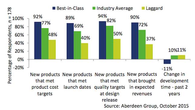
In late 2015, we collaborated with the Aberdeen Group on a study aimed at identifying the capabilities shared by the most successful PCB design companies. You can read the report in full here – it’s well worth your time. For now, though, here are some of its findings that are particularly relevant to this discussion.
Figure 1 shows the metrics used to define companies that were best-in-class. Given my theme here, the important (and perhaps the only surprising) number is the one on the far right. Only best-in-class companies had managed to reduce development times in the last two years.
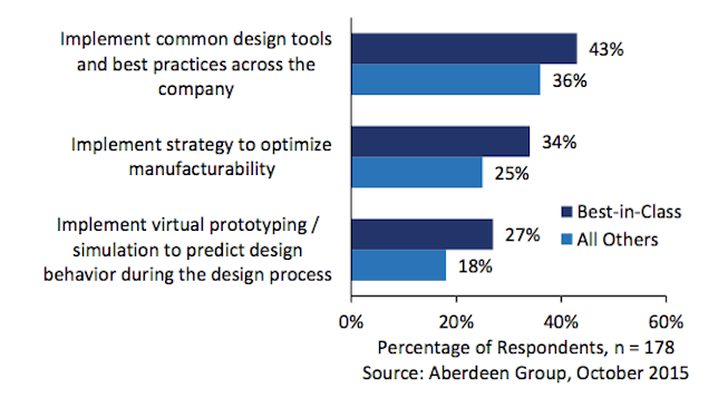
Figure 2 then shows the most effective actions companies had taken to cut time-to-market. The data highlights the importance of using the best available tools within a defined, optimized and collaborative internal design process.
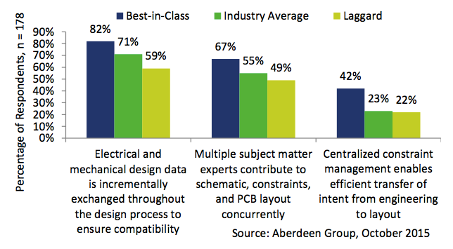
Finally, Figure 3 shows how collaboration leads to better finished products.
‘OK’, you might say, ‘That’s what the cool kids are doing. But how do I match them?’
Alongside the report, Aberdeen has developed an online benchmarking questionnaire. It leverages the findings from the study – which featured 175 active PCB design houses – and allows you to rate your own core design practices against the sample. Aberdeen will also come back with some recommendations on how you could improve your processes.
I’d encourage anyone who hasn’t undertaken this exercise to do so. But remember this also: Shared best practices are only a starting point. One lesson that design tool vendors have learned – painfully, you could say – is that software which attempts to apply a one-size-fits-all design methodology too deeply never really works.
Every company has its own culture and, quite possibly, closely-guarded internal practices that give it a particular competitive advantage. Any methodology will require customization.
But, going back to my original point, it is probably the case that technological complexity and a focus solely on technological solutions has diverted attention away from design processes. To get back on track, it is worth looking at what your rivals are doing to see if there are some basic strategies shared by the most successful and how they could be applied to your own company.
Click here to learn more about the winning projects in the Mentor Graphics 2015 PCB Technology Leadership Awards and for a further overview of market trends they illustrate.
 David Wiens is Business Development Manager for the System Design Division at Mentor Graphics.

