Using HAPS to streamline IP to SoC integration
About 70% of ASIC designs use FPGA-based prototyping for system validation. The technique’s rising popularity is being driven by two trends.
The first is an increase in the number of software elements, such as applications, drivers and firmware, which need to be developed and validated in SoCs.
The second is the growth in overall hardware complexity when a design combines IP from multiple sources, advanced processors and high-speed external interfaces.
Can traditional FPGA-based prototyping boards scale to meet the challenge presented by the combination of these two trends? From our perspective, we’ve reached something of an architectural traffic jam.
Traditional prototyping boards use a structured architecture. This has predefined interconnects which, in the current design environment, limit a user’s ability to do early IP validation and then port that IP to a full prototyping system.
Traditional architectures and traffic jams
Think first of an FPGA-based prototyping board as being like a large city, and then of the infrastructure such a city requires.
Each functional logic block is a complete, self-defined neighborhood. It is connected to other neighborhoods by freeways. But the freeways were built before the neighborhoods, in some cases before the neighborhoods had even been fully planned. Each freeway might have space to carry a lot of traffic (perhaps hundreds of signals) between each neighborhood, but these roads are not flexible, moveable, or expandable.
Moreover, this infrastructure perhaps worked when the neighborhoods were founded and all their users stayed in their original places – but nothing stays the same forever. If, over time, nearly everyone who lives in one neighborhood starts working in another, some of the city’s arterial routes will be overwhelmed with traffic while others progressively empty. To add to the existing challenge, there’s no easy way to divert the traffic, or expand the freeway.
This brings us back to the prebuilt interconnects between blocks in traditional prototyping systems. For example, there might be 200 interconnects between block A and block B, and 200 between block B and block C. The user defines the logic in these blocks, but not the interconnects. So, when the next-generation chip needs 400 signals between block A and block B, there’s no way to shift the interconnects between block B and block C, and no easy way to integrate an IP prototype if the pins don’t align.
A flexible system architecture
What we need to meet today’s design challenges is a prototyping architecture with flexible I/O ports that are defined by the user. Prebuilt interconnects lead to congestion. Such an architecture can address the changes now occurring from one design to the next. It enables SoC validation teams to reuse the FPGA-based prototyping system with a variety of design styles and projects. This is the philosophy that has been adopted for the development of the Synopsys HAPS-70 prototyping system.
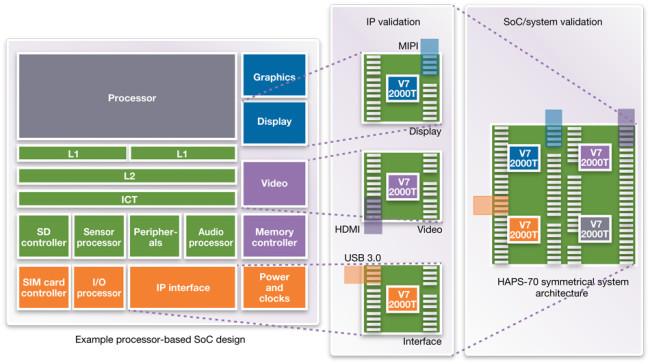
The HAPS-70 architecture is completely symmetrical, starting with the S12 system. It supports up to 12 million ASIC gates and has more than 1,000 definable ports on each board. With so many more ports, the number of configurations available exceeds what any design today will need, even at the entry level. The HAPS-70 system also scales to the S144 system, which supports up to 144 million ASIC gates.
This architecture means that your ‘city’ can have fully configurable interconnects, according to need. This flexibility also means that IP developers can create powerful FPGA prototypes using a smaller system and validate any specific software drivers, applications and firmware on them.
The design in Figure 1 contains multiple IP blocks from third party vendors or legacy designs that are already fixed; high-performance, external interfaces based on standard protocols; and multiple ARM processor cores. With a flexible architecture, even at this stage users can undertake early IP validation to check the MIPI, HDMI, and USB 3.0 interfaces in parallel.
Figure 1 HAPS architecture streamlines IP to SoC integration (Source: Synopsys)
Advanced verification
When the individual IP validation is complete, the implementation and scripts used to optimize and validate the IP can be reused in a larger HAPS-70 system for the full SoC-level FPGA prototype. The SoC validation team can then focus on interconnects between various blocks at the SoC level, as the individual blocks have already been validated. This dramatically lowers bring-up time.
With the need for platforms that support IP- and SoC-level designs for system validation, users are already driving the market toward common, transferrable hardware platforms. Any mix of hardware prototypes that can only be used for one kind of project is no longer enough.
But hardware/software design teams looking to maximize software development time without sacrificing silicon or system quality should also seek out FPGA-based prototyping systems that offer a flexible I/O architecture. Today’s challenges demand nothing less.
Author
Neil Songcuan is a senior product marketing manager, who is responsible for the FPGA-based Prototyping Solution at Synopsys. His experience includes the areas of semiconductor, hardware-assisted verification and system validation. Neil has held various marketing management positions with Synplicity, Mentor Graphics and IKOS Systems. Additionally, Neil worked in customer marketing and application engineering roles with Altera Corporation. Neil holds a B.S. degree in Electrical Engineering from San Jose State University.
 Neil Songcuan is a senior product marketing manager, responsible for the FPGA-based Prototyping Solution at Synopsys.