Using advanced IP to build SoCs for hyperscale data centres
SoC suppliers building the key components for hyperscale data centres need access to the latest IP to handle functions such as PCIe, DDR5, cache coherency, NVMe SSDs, and the highest-bandwidth Ethernet implementations.
An increasing amount of computing work is moving from traditional to hyperscale cloud data centres. According to Cisco’s Global Cloud Index, by 2021, 94% of all workloads and compute instances will be processed in cloud data centres (Figure 1). The use of private (rather than public) hyperscale data centres is expected to grow 11% a year from 2016 to 2021.
Although the largest public cloud providers build their own rack-scale systems, private cloud providers typically use converged infrastructure (CI) or hyper-converged infrastructure (HCI) systems to boost efficiency and cut management costs. These approaches make it easier to rapidly deploy large systems with automated configuration and control, and to virtualize compute, storage, and networking operations.
Figure 1 The distribution of Cisco workloads between traditional and cloud data centers (Source: Synopsys)
The system-on-chip (SoC) suppliers who provide the key components for the underlying hardware need optimized processor architectures and the latest IP to handle functions such as PCI Express (PCIe), DDR5, cache coherency, NVMExpress (NVMe) solid-state drives (SSDs), and the highest-bandwidth Ethernet implementations.
Improving performance with NVMe SSDs and PCIe-based accelerators
For example, SSDs can be used in servers to act as fast cache, by running the NVMe protocol over a PCIe interface to the CPU. This improves server efficiency and avoids having to access the data on an external storage device. NVMe SSDs running over PCIe are useful for cloud-based database servers that have to respond to high volumes of queries.
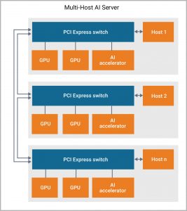
CI and HCI systems also use low-latency PCIe switch architectures to connect host processors to the GPUs and hardware-based accelerators used to optimize deep-learning algorithms (Figure 2). For applications that need cache coherency, the Cache Coherent Interconnect for Accelerators (CCIX) protocol, which is built on top of the PCI Express protocol stack, provides a high-speed connection between host processors and hardware accelerators. CCIX ensures that the system sees a single memory space, by defining commands to update all components across the system when memory is updated. The protocol runs at 25Gbit/s now and will soon run at 32Gbit/s, and works with switch topologies, direct- and meshed-connection strategies.
Figure 2 Multi-host AI server based on PCIe switch architecture (Source: Synopsys)
Optimizing applications with high memory performance
Converged compute, storage, and networking systems need fast access to DRAM to run virtual applications on host processors, which is why DDR5 and HBM2 DRAMs are becoming popular. DDR5 memories can run at up to 4800Mbit/s, interfacing with multiple dual in-line memory modules over channels up to 80bit wide. DDR5 also has reliability, availability, and serviceability features, such as inline or sideband error-correcting code, parity, and data cyclic-redundancy checking, which make it useful for high- reliability applications.
The high-bandwidth memory (HBM2) standard for packaging and interfacing to multiple memory dice enables very high bandwidths, and a lower energy cost per bit of data accessed than DDR5 DRAM. SoC architects use HBM2 for high-bandwidth applications, DDR5 for high capacity, or a combination of them for applications that need both characteristics.
Simplifying data centre networks
Traditional enterprise data centres use a tree-based network topology enabled by switched Ethernet and VLAN tagging. This topology only defines one path to the network, which has traditionally handled north-south data traffic between servers.
CI and HCI systems use a two-tier, leaf/spine architecture with 25, 50, 100, or 200Gbit/s Ethernet links to distribute workflows among many virtual machines. The latest 400Gbit/s Octal Small Formfactor Pluggable multi-mode transceivers use eight 56Gbit/s channels, implemented using PAM-4 PHY IP blocks, to support networks running at up to 400Gbit/s by providing multiple 56Gbit/s leaf/spine links. A shift to 112Gbit/s PAM-4 Ethernet links will enable a move to 800Gbit/s Ethernet applications.
CI and HCI systems may also use a software-defined network strategy to simplify network management, by decoupling network control from the data path. The OpenFlow stack provides a consistent software environment, which means SoC designers can rely on OpenFlow-managed data movement throughout private cloud data centres. This makes it easier for users to provision their networks virtually, without having physical access to the network’s hardware.
Summary
CI and HCI systems integrate the compute, storage, and networking aspects of a hyperscale data centre, replacing what can otherwise be a diverse set of systems and management tools. At the same time, many enterprise data centres are turning into private clouds that use virtualization to run more workloads on fewer physical servers.
Building this kind of converged system demands access to the latest processor architectures, connectivity, memory technology, NVMe SSD interfaces, and cache-coherent accelerators, all expressed as semiconductor IP designed for easy integration into complex SoCs.
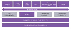
An example of the kind of SoC that can be built with this IP is illustrated in Figure 3, which shows an advanced AI server SoC that has a host processor, multiple accelerators, hardware security features, as well as sophisticated memory interfaces and connectivity options.
Figure 3 AI acceleration/server SoC (Source: Synopsys)
Synopsys has a comprehensive portfolio of silicon-proven IP that enables designers to develop SoCs for use in CI and HCI systems. Synopsys’ DesignWare Interface, Processor, and Foundation IP is optimized for high performance, low latency, and low power, and can be instantiated on 16nm to 7nm finFET processes.
Author
Ron DiGiuseppe is a senior product marketing manager Synopsys.


