The new kid on the USBlock: introducing SuperSpeed 3.0
The USB 3.0 specification was approved in 2008 and the first certified products to take advantage of its SuperSpeed (5Gbit/s) were launched at January’s Consumer Electronics Show in Las Vegas. As more support for the standard becomes available, engineers will find themselves considering the specification’s implementation on all types of system projects during the course of the year. This article provides a high-level overview of USB 3.0’s potential, its limitations and its new features (including power management).
In the beginning, there were Low Speed and Full Speed USB with their 1Mbit/s and 12Mbit/s signal rates respectively, and they worked well enough for the needs of 1996. Four years later, USB 2.0 arrived at 480Mbit/s. A few years later still, the USB standard was extended with On-The-Go functionality that allowed two devices in the field to connect without the need for a host (typically a PC). And the next step after that was Wireless USB, but it has not proved quite as successful.
Coming up to date, 2008 saw the approval of SuperSpeed USB—aka USB 3.0—with a potential speed of 5Gbit/s. It still stands at an early point in its adoption curve, so it is timely to review its capabilities, its limitations and its potential as engineers increasingly consider its integration within their system designs.
Real-world speed
The signaling speed of USB 3.0 is 5Gbit/s, though its actual transfer performance is limited by a number of factors. The 8/10bit encoding used to equalize the DC current flow in copper wiring cuts the maximum possible speed to 4Gbit/s. Then, the overhead needed for headers and mandatory link layer commands shaves it further to 3.76Gbit/s. Finally, additional overhead for interpacket gaps and additional link commands brings things down to an effective data rate of 3.69Gbit/s (this translates into 440Mbyte/s). This speed is unidirectional, but SuperSpeed does support dual-simplex transfer, so it is simultaneously available to both the transmit and receive streams, giving 2 x 440Mbyte/s paths as opposed to the 40Mbyte/s half duplex transfer capability of USB 2.0.
Cable and connector
To achieve high transmission rates, both the cable and the connectors have been modified. There are now two additional twisted, shielded differential pairs for the transmit and receive links. At the same time, USB 2.0 elements have been retained, such as a data pair (D+/D-) and power plus ground lines.
To prevent electromagnetic interference (EMI) and improve signal integrity, USB 3.0 cables are shielded. Consequently, they are thicker, less flexible and also more expensive than USB 2.0 cables.
To ensure compatibility of the interconnect, the USB 3.0 Standard-A connector is visually almost identical to that for USB 2.0 Standard-A. The differences are inside the plug. In the back, there are five extra connectors for 5Gbit/s transmit and receive link pairs plus an additional ground. In the case of the Standard-B connector, the difference is much more immediately conspicuous. There is a hump-like portion added to accommodate the SuperSpeed pins. For the Micro-B connector used in mobile devices, the SuperSpeed USB 3.0 pins are placed alongside those for the USB 2.0 part.
Because of this construction, the USB 3.0 Standard-A plug is mechanically compatible with the USB 2.0 receptacle and vice versa. But in the case of the Standard-B connectors—both regular and micro—the USB 2.0 cable can be hosted by a USB 3.0 port, but not vice versa. The various types of connectors are shown in Figure 1.
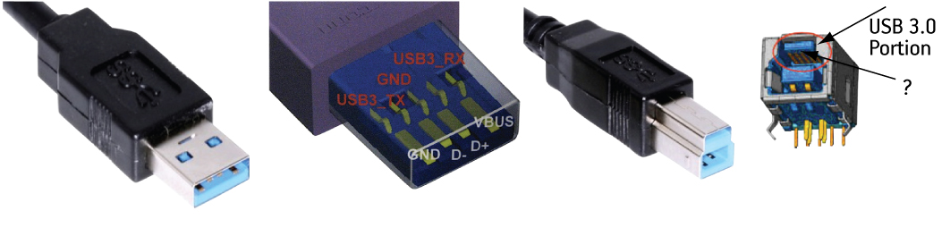
Figure 1
USB 3.0 connectors
Source: Intel
Dual bus architecture
SuperSpeed USB preserves the bus structure topology of earlier iterations of the technology, so there are still seven tiers of devices/hubs with a host at tier one and a root hub at tier two. The idea behind USB 3.0, as with previous revisions of the specification, has been to ensure backward compatibility and support both SuperSpeed and High Speed transfer rates.
So, all certified hubs and hosts need to support both paths—SuperSpeed as well as the legacy paths (HS/FS/LS). Certified peripheral devices must also support both speeds even though they cannot operate in more than one mode at any time. The minimal required support for a non-SuperSpeed rate in a SuperSpeed-enabled peripheral is to request connection to a SuperSpeed port.
Of course, having a USB 3.0 device working at SuperSpeed requires it to be connected to a compatible host through a compatible hub using an appropriate cable. While multiple connections are physically possible, the speed will always be limited to that of the device enabled for the slowest specification—if a SuperSpeed and a High Speed device are connected, performance will be only High Speed. The same applies if a USB 3.0 device is connected using a High Speed cable or via a High Speed hub.
Dataflow
Comparing the data flows for USB 3.0 and USB 2.0 highlights huge differences in the standards (Figure 2). In USB 3.0, data transfers and handshakes are not intermingled with each other because of the separated transmit and receive lines. Data packets and respective handshakes are sent on different pairs. This eliminates losses in bus time consumed by propagation delays and turnaround time in USB 2.0 implementations of a single transmission pair.
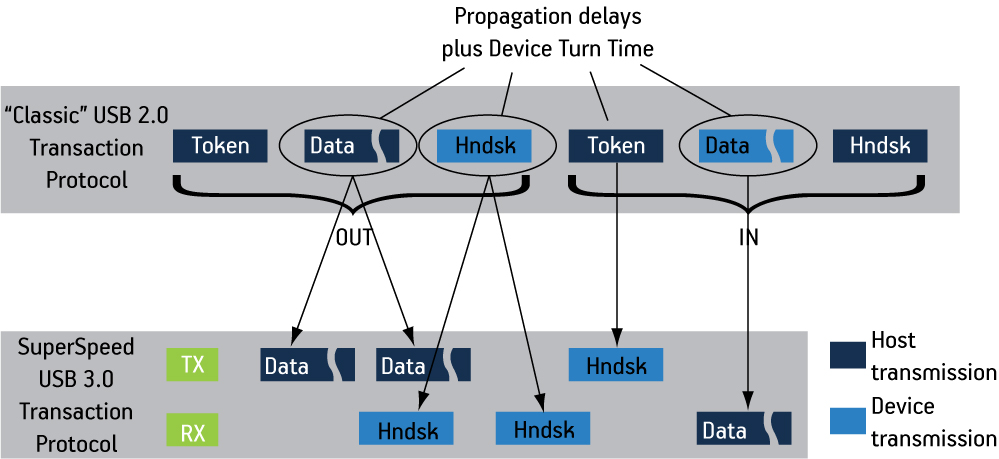
Figure 2
USB 2.0 and USB 3.0 transaction protocols
Source: USB-IF
This advantage of USB 3.0 has been used in endpoints supporting burst transmission where the parties exchanging data do not need to wait for each other before sending consequent packets, and also do not need to give up transmission line capacity to wait for a handshake packet. In regular non-burst operation, parties still need to wait for a handshake packet after sending each data packet.
Architecture
The architecture of USB 3.0 (Figure 3) is significantly more complex than that of USB 2.0, so an attempt to simplify the new standard’s management has been made by organizing it into four layers:
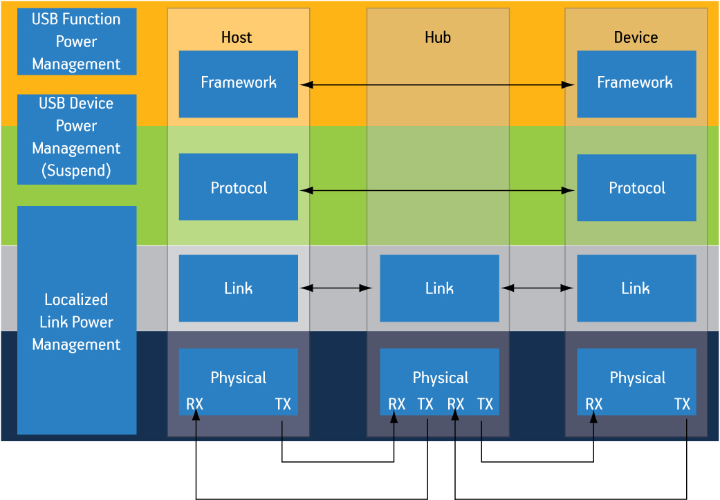
Figure 3
USB 3.0 architectural overview
Source: USB-IF
- Physical
- Link
- Protocol
- Device/host
The first two layers are based on PCI Express, providing a further entry point for the many engineers already familiar with that standard.
Physical layer
The physical layer transfers information over the physical media in the smoothest and the least distracting way. There is an 8/10bit encoder/decoder to equalize DC load; a scrambler/descrambler and spread clock & data recovery (CDR) to reduce electromagnetic interference; and elasticity buffers/skips to prevent any data stream interruption due to clock synchronization.
There is then a further element, low frequency pulse signaling (LFPS), that is not present in PCIe and which merits a little more attention. Connectivity at 5Gbit/s requires a considerable amount of power. Consequently, staying connected to just monitor high-speed traffic would be inefficient in low-power modes, and wholly unacceptable for low-power-oriented devices and applications. LFPS has therefore been added to provide power management signaling. It is a signal transmitted over the media that oscillates at a relatively low frequency, in a range of 10MHz to 50MHz.
Link layer
The link layer is a low-level connection management layer. The link layers of connected parties, which are called ‘link partners’, take care of various events and exchange some commands to control the power states of the link. They ensure the error-free transmission of packet headers (the data payload is managed in the protocol layer) and provide flow control. Event management covers such situations as connection negotiation (e.g., a training session) and disconnection.
Link-layer logic is also responsible for correct framing of the transmitted packets, detecting frames of the received packets and also passing through all protocol-layer packets. Another important part of the link-layer operation is the negotiation of low power modes. If a connection is to go into a low power state, both participants must be appropriately transitioned.
Protocol layer
While the link layer manages connections between partnering links at the ends of the physical connection, the protocol layer sits on top of it and takes care of communication between a host and a device. As in USB 2.0, communication between the host and the device is based on data exchange in the form of pipes wherein information is sent to and from peripheral device endpoints.
USB has always been a host-centric protocol; that is to say that data exchange is initiated by the host. This differs from other protocols like IEEE1394 (FireWire) for example, where any node can send data to any other on the bus. The host-oriented model has been preserved in USB 3.0 with a slight difference; there is no longer a polling of ‘not ready’ devices, as happened in USB 2.0—more about this can be found in the ‘Power Management’ section below.
All data and control sequences are conveyed to the host directly through all hubs in the path and vice versa—device-directed packets are routed straight to the targeted device. There is only one packet in USB 3.0 that goes to all devices that are not idle or suspended. It is the timestamp packet used to synchronize all devices on the bus.
This is a further advantage of USB 3.0 over USB 2.0, where all traffic from the host is transmitted to all connected devices, causing them all to be busy while they check the device address. USB 3.0 thereby reduces activity at the device side. However, there is also a disadvantage for hubs as they need to be aware of their downstream connection tree and route packets accordingly.
The primes of the data exchanged through the pipe between the host software and device endpoint have been preserved in USB 3.0. There are still four transfer types through the pipe: bulk, control, interrupt and isochronous.
A feature called ‘streams’ has been added to the bulk transfers. A dedicated field in the packet header, called ‘StreamId’, is used to distinguish series of data being transmitted to or from an endpoint. Using this feature, media storage devices can service more than one single file transfer at a time and assign various priority ratings to each transfer.
Device/host
The device—or host—is a functional layer that sits on the top of the three described above. It can have a single function (e.g., a single interface offered by a computer mouse), multiple functions (e.g., a composite device such as a headset with a microphone) or be a hub (e.g., a compound device with a set of permanently attached devices).
The host implements its functionalities through software and a host controller. It needs to implement both transmission paths—SuperSpeed and non-SuperSpeed—to be able to service all types of devices. It also simultaneously controls and manages transfers over the bus using the appropriate speed path. Enumeration, control operation, data flow control, statistics and power supervision are all tasks implemented in the host.
Power management
Because the market demand for effective power management has increased over the last few years, it forms a major part of the USB 3.0 specification.
First, device polling has been eliminated and replaced by the ‘ERDY’ notification. When the device is not ready to transmit or receive the data it sends a ‘Not Ready’ packet, after which the host stops asking the device for transmissions and waits until the device reports its readiness using ERDY. Broadcast packet transmission through hubs has also been dropped. Finally, additional modes of operation have been introduced.
The first two options reduce unwanted traffic between connected devices and disable connections during periods of inactivity. The additional modes then enable more efficient power management during periods of inactivity, and allow the system to respond to traffic in a shorter time. There are now four modes:
- U0 – Link active: normal working state, full power.
- U1 – Link idle: fast exit, transmit and receive clock can be disabled, but clock generation needs to operate, state exit latency in the magnitude of microseconds
- U2 – Link idle: slower exit, physical layer clock generation can be switched off, state exit latency in the magnitude of milliseconds
- U3 – Link suspend physical layer power can be switched off.
There are significant differences to the ways in which devices can enter these states. Entry into the U1 and U2 states can be triggered by hardware (inactivity timers) or software (appropriate drivers). If one of the link partners wants to go into a low power state, it tries to negotiate it and the other link partner can accept the request or reject it. Rejection could happen if there is some ongoing activity that will require a transmission within a short period of time. The U3 state can be triggered only by managing software on the host side, and the device always needs to accept the request to enter the U3 state.
The LFPS mechanism described earlier is used to signal that a device wishes to exit from any of the low power states.
Software
As USB 3.0 integrates High Speed and SuperSpeed functionality under the same hood, the software layer also needs to be able to manage these two standards. The biggest challenge here is the implementation of protocol software, ensuring compatibility with different devices. Microsoft foresaw this challenge and has postponed host software support for USB 3.0 until the release of Windows 7 Service Pack 2. It hopes to thus avoid suggesting that ‘plug and play’ capabilities will be available when they are not and thereby avoid complaints from users.
Conclusion
The table in Figure 4 (p. 53) provides an overview and comparison of the main features and differences between USB 2.0 and USB 3.0. Armed with this information, engineers can aim to take realistic advantage of the speeds and efficiencies offered by USB 3.0 as a greater range of product, services and intellectual property also becomes available.
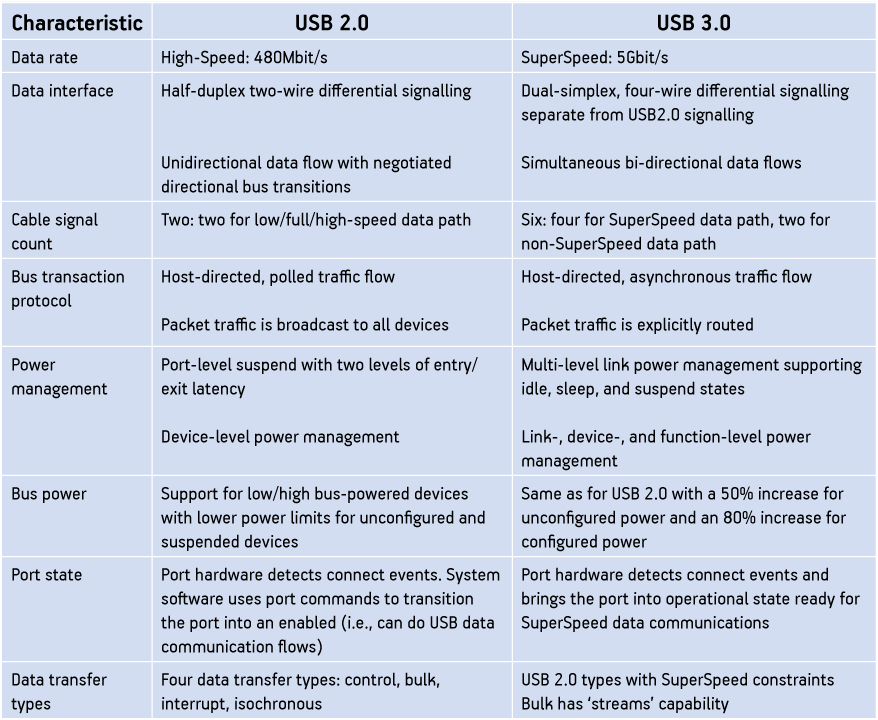
Figure 4
Feature comparison for USB 2.0 vs. USB 3.0
Source: Intel/USB-IF/Evatronix
Bibliography
Conference proceedings of SuperSpeed USB Developers Conference; San Jose, California; November 17-18, 2008
Evatronix SA
ul. Przybyly 2
43-300
Bielsko-Biala
Poland
T: +48 33 499 59 15
W: www.evatronix-ip.com