Strategic considerations for emerging SoC FPGAs
This white paper describes the emergence of SoC FPGAs, the drivers behind their market, and proposes some strategic considerations for executive management and system designers when choosing these devices.
Semiconductor devices that integrate FPGA fabric, hardened CPU subsystems, and other hardened IP—SoC FPGAs—are poised to proliferate broadly in their usage.
SoC FPGAs build upon the decade-long availability of soft-core CPUs and other soft IP that have been used to build systems on FPGAs. A mix of technical, business, and market forces is now converging to create a tipping point for the technology. In response, vendors such as Altera, Cypress Semiconductor, Intel, and Xilinx have announced or are now shipping SoC FPGA devices.
In the SoC FPGA era, systems designers should consider the following key strategic questions when choosing these devices:
- Which devices will experience a “platform effect” that leads to a self-reinforcing cycle of vendor, ecosystem, and customer development?
- Which devices will support IP reuse across the broadest array of options?
- Which FPGA technology allows for the maximum cost and performance effectiveness?
The tipping point for SoC FPGAs
The initial decade of integration across FPGAs and CPUs had both successes and failures. The first wave of explicitly branded
SoC FPGAs had limited commercial success. At the same time, the use of soft CPUs within more ‘traditional’ FPGAs did secure broad acceptance, indicating that there was a fundamental market desire for bringing together the two technologies.
Several factors are now reshaping the market and have helped bring us to the tipping point for wider adoption of SoC FPGAs. Foremost among these are:
- computing power efficiency
- FPGAs on leading-edge process technologies
- growing adoption of FPGAs in embedded systems
- the economics behind Moore’s Law
- consolidation in CPU architectures
Computing power efficiency
The evolution of computing is toward parallelism, with the near-term focus on processors shifting from higher power, single-core implementations toward multicore implementations. As part of the allied quest for higher performance at lower levels of energy consumption, the idea of using FPGA logic as hardware accelerators for CPUs is attracting more attention.
A monolithic SoC FPGA system maximizes power efficiency and software partitioning flexibility. SoC FPGAs allow hundreds of data signals to connect different functional areas, thus enabling 100Gbit/s bandwidth or greater at nanosecond-level latencies. This represents orders of magnitude in improvement across both performance and latency over discrete implementations. Furthermore, monolithic integration permits sharing of memory controllers, allowing high-bandwidth memory access for hardware accelerators.
This increased performance and memory access enables the use of the FPGA for finer-grained accelerators to address a broad class of computing requirements. Because hardware accelerators can have more than 1,000 times the power efficiency of CPUs, designing for SoC FPGAs creates significant potential for an improved approach to power efficient computing, beyond what simple multicore parallelism can achieve.
FPGAs on leading-edge process technologies
In the year 2000, state-of-the-art FPGAs were built on 130nm process technology, while state-of-the-art CPUs were built on 90nm. Because more advanced CPUs were available, the appeal of the first generation of SoC FPGAs was somewhat dampened. Today, however, leading-edge FPGAs are targeting 28nm process technology, which relatively few commercial CPUs or
ASSPs use—or are likely to use—in the near future. The process technology advantage of FPGAs significantly increases the market potential of—and the inclination of vendors to invest in—these integrated devices, as designers do not need to compromise on the CPU’s capabilities, as illustrated in Figure 1.
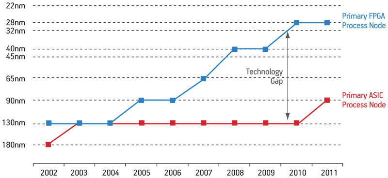
Figure 1
FPGAs move to leading-edge process technologies
Source: Altera
Growing adoption of FPGAs in embedded systems
In the year 2000 FPGAs were still relatively expensive given the budgets for most embedded applications, and as a result were used less frequently than their CPLD or PAL counterparts. In the last decade, however, SRAM-based FPGAs have ridden the CMOS cost reduction curve. EE Times’ 2010 survey of the embedded market found that nearly 50 percent of embedded systems also contain FPGAs.
Because one of the major appeals of SoC FPGAs is the reduced cost of these devices compared to discrete implementations, there is a large native market from which silicon vendors already see themselves achieving extremely solid returns on investments today.
The economics behind Moore’s Law
Moore’s Law is becoming more and more expensive to support. Fabrication facilities that build advanced CMOS semiconductors cost anything from $6B to $10B to build. Per project design costs are at $40M and rising, so any new chip must recover $100M in gross profit to conform to a typical profitability model where 20% of revenue is spent on R&D.
At typical gross margins of 50%, a firm must capture a market of $200M or more. Outside of consumer electronics, mobile handsets, and PCs, there are few applications of this size. As NRE costs grow even higher for future process technologies, this cost structure will make it even more difficult to economically justify building fixed-function semiconductors. All this suggests that programmable technologies will see increasing adoption, while fixed-function devices—including specialized ASSPs and CPU derivatives—will see less. Because SoC FPGAs have the potential to serve many markets, they are especially well positioned to take advantage of this shift.
Consolidation in CPU architectures
The term ‘embedded processing’ covers a broad spectrum of applications, from extremely cost-sensitive ones that still use 4bit processors, to extremely sophisticated ones based around multicore 64bit machines.
Historically, this breadth in the market has long supported a diverse and fragmented set of processor types, operating systems, and software vendors.
Yet that diversity is markedly different in the year 2011 as compared to the year 2000. For all its size and variety, the general embedded market is moving toward faster and more capable processors—for example, 16bit microcontrollers are already giving way to 32bit CPUs.
At the same time, support for 32bit families is consolidating around four architectures: ARM, MIPS, PowerPC, and x86. The consolidation is due mostly to software commonality and reuse.
As a result, an SoC FPGA that incorporates one of these CPU architectures can address an intrinsically larger market, thereby adding more incentive for vendors to invest in this class of semiconductor.
The platform effect
Products that have an interrelationship in terms of their adoption between producers, users, and their ecosystem tend to exhibit what is called a ‘network’ or ‘platform’ effect.
The basic tenet of the platform effect is that the more use a particular product, or standard, attracts, the more valuable it becomes to members of the user base and ecosystem. As a result, the members of the user base and ecosystem then invest more in the technology, thus attracting more use and creating a self-reinforcing cycle. Familiar examples include PCs, video recording formats, and social networking sites.
In general, product categories that have the innate possibility to operate in a self-reinforcing cycle have a stronger tendency to evolve according to the market’s needs, as each actor in an emerging product category looks to maximize ROI. As soon as a potential platform starts to gain momentum, it begins to attract investment, and thus the market dynamic can quickly shift toward that standard.
SoC FPGAs have a strong likelihood to see this platform effect. As they proliferate, there will be a strong desire for users to reuse their FPGA IP and design software know-how across a wider variety of systems. For example, members of CPU ecosystems will prefer to learn as few FPGA development tools as possible, and CPU vendors will prefer to minimize the number of FPGA development tools and technology that they need to know.
As a result, SoC FPGA platforms that support multiple vendors and CPU architectures will be best positioned to trigger the investment associated with this effect, thereby creating the most advantages to customers and ecosystem members who join in its adoption.
Altera’s approach
Altera has launched its “Embedded Initiative” with the intention of creating a multivendor, multi-CPU architecture SoC FPGA platform based on a single FPGA design flow methodology.
The FPGA design flow methodology aims to serve as the basis for a wide variety of SoC FPGAs over time, as well as SoC solutions using soft CPUs and other soft IP. ARM (hardened), MIPS (soft), and Nios II (soft) CPU options are or will be available from Altera, while the Atom E6X5C Configurable Processor devices will be available from Intel.
This integrated approach unites three of the leading CPU architectures and one of the most popular FPGA-based soft CPUs around a single FPGA architecture and design flow.
Fostering innovation
The integrated approach to FPGA design flow methodology is intended to stimulate the ecosystem so that leading processor architectures will invest in a single FPGA platform and tool flow, thus creating an enriched set of tools, application software, operating system software, and professional expertise.
With the investment of hundreds of collective, global ecosystem members, this FPGA platform and its growing list of tools, software, and IP could become increasingly useful and important to system designers, presenting them with the value proposition that will trigger their adoption, and thus fuel the virtuous platform cycle.
Providing tools and IP
A key component of Altera’s multivendor platform is the Quartus II software flow for programming FPGA logic. It includes the Qsys system integration tool, which features Altera’s second-generation switch fabric technology that can be used to accelerate soft IP development, reuse, and integration.
In addition to Altera’s existing Avalon Memory-Mapped (Avalon-MM) interface and data path bus interface specification, Qsys will also support the ARM AXITM standard, which enables an automated ‘mix and match’ approach to integrating Avalon-based IP with AXI-based IP. Qsys supports design reuse and in-system verification across the entire common platform for ARM- and Intel-based SoC FPGAs, as well as MIPS and Nios II soft CPU SoC implementations.
Tailoring a 28nm portfolio
Altera’s 28nm FPGA portfolio delivers a comprehensive set of device options tailored to customers’ diverse design requirements, across a variety of end application requirements.
High-density Stratix V devices are optimized for performance. High-volume Cyclone V devices are optimized for cost. And mid-range Arria V devices provide a balanced mix.
Altera’s newest SoC FPGA will contain an advanced processor block based on the ARM Cortex-A9MP core, as shown in Figure 2 (p. 51).
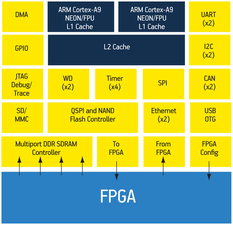
Figure 2
The Altera SoC FPGA architecture
Source: Altera
The Altera SoC FPGA architecture will feature a broad array of hardened IP within the ARM-Cortex A9 subsystem, as well as high-performance multiport memory controllers for maximum memory bandwidth.
High-bandwidth, low-latency interconnects between the FPGA and the CPU subsystem will allow for high-performance applications and efficient FPGA hardware acceleration.
Advanced internal switch fabrics will support efficient data throughput, as well as highly productive in-system observability and debugging.
When combined with Qsys, the Quartus II software, and ARM Connected Community software tools, this device will represent a highly cost-effective system design option that leverages standard tool flows for maximum productivity, and offers significant new development and verification possibilities.
Conclusion
The era of SoC FPGAs has begun. These devices have reached a tipping point driven by key economic, technical, and market forces, and numerous vendors have already announced or are shipping such products. Executive management and system architects should carefully consider platform effect, IP reuse, and FPGA process technology benefits when evaluating system solutions.
Altera has partnered with leading CPU vendors ARM, Intel, and MIPS, to provide a common FPGA platform for SoC FPGA devices and soft CPU solutions. This partnership will allow the industry’s most widespread CPU architectures and their ecosystems to inherit the same advanced FPGA design flow, thereby maximizing the IP reuse and flexibility within this platform.
This integrated approach creates a platform effect that will foster growth and development on this platform, as well as on the supporting CPUs and their ecosystems.
Chris Balough is senior director for Software, Embedded, and DSP marketing at Altera.
Altera
101 Innovation Drive
San Jose
CA 95134
T: +1 408 544 7000
W: www.altera.com