Meeting yield enhancement challenges
Nanometer scaling severely inhibits the path to achieve sustainable yield. In response more responsibility for forecasting potential failures must shift to design for manufacturing (DFM) methodologies that can be applied early in the design process. Yet, while these hold much promise, manufacturing test and failure analysis remains at the forefront of determining why chips fail.
Indeed, those chips that fail production offer a goldmine of information, which can provide valuable insight into defects and failure mechanisms. Developing a methodology that enables diagnosis of more than small samples of failing devices can thus greatly improve yield learning.
The ITRS roadmap makes the importance of better detection clear when it lists the four main challenges an effective yield enhancement program must address:
- DFM and design for test (DFT) techniques are needed to better understand systematic mechanisms limited yield (SMLY).
- High-speed, cost-effective techniques are needed to detect ever smaller features.
- A high detection rate is necessary to monitor where process variation ends and defective behavior starts.
- Failure analysis tools and techniques are needed to identify causes of failure where there is no visual defect.
These challenges motivate us to take a fresh look at how manufacturing failures are processed. Historically, manufacturing test has primarily sought to prevent defective parts leaving the fab. Until recently, very little effort has gone into looking at the root causes of these failures, except for small samples.
At larger geometries, small samples sufficed because most defects were random in nature.
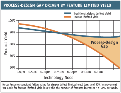
Figure 1. Below 180nm, systematic feature-related yield loss becomes a critical issue.
But at smaller geometries, more systematic and interconnect-related defects are prevalent (Figure 1). Relying on small samples lengthens yield-learning cycles and introduces significant risk as new process technologies are applied. Harnessing information buried in previously ignored failing devices allows us to take prompt corrective action to bring about a more predictable yield ramp.
Invisible faults wreak havoc
This is the age of subwavelength lithography.With feature sizes below the wavelengths of light being used for traditional optical lithography, the industry has turned to reticle enhancement technology (RET). This uses modifications to the mask data such as phase shifting and optical proximity correction (OPC) to extend the range of optical lithography.
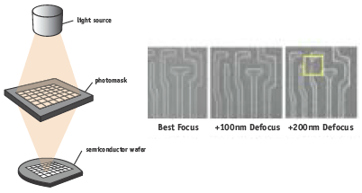
Figure 2. Lithography variations in focus/dose and their impact on a circuit.
Due to the precision of the optics and the accuracy of the optical correction methods, subwavelength lithography itself introduces new and more systematic type defect mechanisms. Even where RET can perfectly adjust a mask to create the targeted layout, variations through the process window can cause distortions in the printed layout that lead to systematic defects (Figure 2).
It is not only the RET modifications made to masks that create differences in the way devices fail. New materials, such as copper, also have a dramatic impact. Dishing effects during chemical mechanical polishing (CMP) can similarly cause higher defect rates. Interconnect defects tend to be closely related to the physical layout. Two lines that run close to each other have a higher probability of having a conductive or resistive bridge form between them than two that are widely spaced. Single vias have a higher probability of failure than double vias.
While these are simple examples, there are many more complicated examples of potential failure mechanisms that can be caused by complex interactions between physical features and the fabrication and lithography process. These cause defect mechanisms that are in many cases non-visual (e.g., a voided or open via) and can only be detected through electrical test. Due to the increasing incidence of such defects, a critical component of any effective defect isolation strategy for nanometer designs needs to be more thorough tests that specifically target these new failure mechanisms.
Defect detection
The first step in yield learning
The quality of shipped semiconductors is directly related to yield. The typical measure of shipped quality is the defect-per-million (DPM) rate. This measures how many defective devices are not detected during manufacturing test. Logically, the escape rate for wafers with poor yield is higher. As companies move to smaller technology nodes with lower initial yield, additional and more effective tests must be added in manufacturing to control the quality level. Furthermore, defective devices must first be effectively screened out during electrical test so that they can be used for yield learning.
The traditional fault model was built around stuck-at tests and focused on the logic gates. The assumption of the stuck-at model was that a test pattern could quickly reveal whether a logic gate was broken by watching its behavior based on switching its inputs. As long as the gate was accessible from I/O pins or through a scan chain, it could be tested. Once each pin on a gate was tested any fault (or failure mechanism) for that gate was marked as detected. This is no longer sufficient. Defect mechanisms in nanometer designs are often subtle interconnect defects that may result in parametric or speed-related failure and that might only fail under certain conditions.
Take, for example, a bridge or short between two adjacent signals on the same layer. Depending on the behavior of the short and the value of the net that the signal is shorted to, a static stuck-at test may not detect the failure. Furthermore, if the bridge is highly resistive in nature the failure may only be observable under high-speed operation.
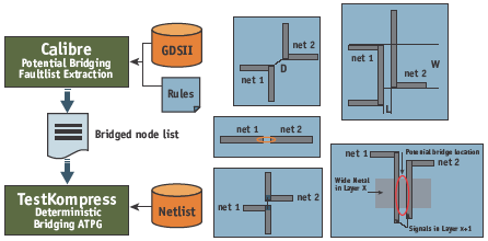
Figure 3. DFM-oriented tests extract potential failures from layout and target tests for those features.
Many of these defects depend on the relative and absolute positions of nets and interconnect features. Design for manufacturing (DFM) rules or recommendations are now commonplace for nanometer design. They indicate what can be done to the physical design to help improve yield. From a test perspective, they also indicate the more likely defect sites. DFM-oriented test is a new methodology that uses DFM recommendations and guidelines to extract from layout the most likely defect locations and types, and then applies specific tests for those defects and locations. Using this methodology, specific tests for bridging or open types of defects can be targeted at those features most likely to suffer from them (Figure 3).
DFM-oriented test not only improves quality or DPM levels, but also provides patterns that are highly diagnosable since it targets specific defects and locations. Failure information from these patterns can provide significant value to the yield learning process. One problem that faces chipmakers is that more types of defect means more tests, and the amount of time and number of test patterns needed is already a problem today. Can the industry work out ways to detect failures without watching the number of test patterns soar? Thankfully, the answer is, ‘Yes’.With embedded compression technology, we have the capability to compress the volume of test data and the test application time by 100X or more (Figure 4).
A yield-friendly, scan-based diagnostics flow
An effective diagnostics flow is needed to leverage manufacturing test for yield learning. The inputs to a scan-based diagnostics system include the logical and physical design data, the test patterns, and failure information from the test process. Valid results depend on having inputs that are consistent. In other words, if the input patterns don’t match the fail log or the design, it is a case of ‘garbage in, garbage out’.
Errors in the incoming data could lead to incorrect results, and thus countless hours wasted in physical failure analysis trying to track down a bogus defect. Re-simulating the pattern inputs with the diagnostic environment provides verification that no changes have occurred from the original ATPG environment and that the patterns do match the design.
However, one of the more difficult steps is converting the automatic test equipment fail log into a consistent format that can be read by the diagnostic tools. Tester differences, extra clock cycles, combinations of functional and scan vectors and variations in when outputs are strobed can lead to incorrect fail file inputs that render unreliable diagnosis results. It is therefore also critical that the incoming failure file is checked to ensure that it matches the patterns and the design.
Additionally, since most testers operate on a cycle basis and not on test patterns, it is important that the diagnosis system import the failure information in this way as well. Accurate test pattern and failure file consistency checking at the input of the diagnostics system ensures that all input data is compatible.
Scan-chain diagnostics
First check the test circuitry
Mainstream manufacturing test relies on scan cells and scan chains to access the internal node of the design. If the scan chains themselves are not working, the required test patterns cannot be applied to the digital logic. Since the flip-flops, scan logic, clocks and enable lines that comprise the scan chain structures can account for a significant portion of the logic, they can also account for a significant portion of the failures. For this reason, the accurate diagnosis of scan chain failures is a first step to understanding yield loss. Diagnosing chain failures requires complex algorithms and can require large amounts of fail data. Collecting enough such data may not be possible during normal production test and may require some off-line processing.
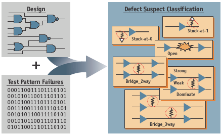
Figure 4. Scan diagnostics takes design information, test patterns and failure information to explain failures.
The first step towards diagnosing chain faults is to look for systematic issues based on the percentage of failures on each chain and each location. If a systematic problem is suspected, additional data can be logged to enable an accurate diagnosis and identify its precise location.
Diagnosis of chain failures involves identification of the type of suspected defects and their location (Figure 4). Suspect defect types include:
- Stuck-at 1 or 0
- Slow-to-rise, slow-to-fall
- Fast-to-rise, fast-to-fall
Logic diagnostics
Identifying and locating defects
Assuming the device passes the scan chain tests, but fails one of the many scan test patterns, accurate diagnosis can provide valuable insight into failure and yield loss mechanisms. Based on the test passing and failing information, logic diagnostics identify potential defect locations as well as suspected defects. Suspect types can be categorized based on the behavior of the failure. Some possible types are:
- Stuck-at 1 or 0 static
- Open type defects
- Signal-to-signal shorts or bridges
- Slow-to-rise, slow-to-fall type defects
This defect identification and classification can aid in locating physical failures and provide valuable insight into overall yield loss. This allows yield improvement to focus on areas that provide the highest return and on rogue lots or wafers that deviate from the norm.
Compressed pattern diagnosis
Embedded compression is quickly becoming mainstream for all nanometer designs. However, one of its frequent drawbacks is a sacrifice of direct diagnostics for compression. It is critical that the compression solution supports diagnosis directly from the compressed responses and the compressed patterns (Figure 6). If diagnostics must resort to a separate set of patterns that are delivered and captured in a “by-pass” mode, rapid yield learning is not feasible. Re-testing wafers with custom pattern sets solely for diagnostics is cumbersome and expensive. The yield-friendly flow must support direct diagnosis from either compressed or uncompressed production pattern sets and fail logs.
Connecting test to design
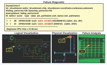
Figure 5. Viewing diagnostics results in physical layout helps isolate failures.
Once defect suspects and types are determined, the next step is to link the failures in the logical domain with the features and locations in the physical domain. Physical information on systematic failures can help pinpoint particular layers, layout features, or die locations to focus debug efforts. Physical diagnosis information can also be combined with in-line data to help filter yield limiting defects from background noise (Figure 5).
During first silicon debug and yield ramp-up, it is not unusual to find physical features that are more prone to fab defects than others. A robust test set may contain patterns designed to identify a mix of stuck-at, transition, path delay, interconnect open and interconnect bridging defects. In many cases due to observed defect rates and DPM requirements, it may be necessary to improve the effectiveness of a given pattern set by targeting additional tests at a specific area or type of defects. Yield-friendly scan diagnostics can help. Based on diagnostics results and links with the physical layout information, specific areas (nets or layers) can be targeted for additional testing based on DFM rules.
An example of this is the identification of possible bridging pair candidates based on DFM rules for net-to-net, via-to-via, or endof- line spacing.With this knowledge, deterministic ATPG bridging patterns can then be created to improve test quality on all nets with suspect features.
Production line diagnosis on volume data sets
In the yield-learning phase, large volumes of data are required to identify yield trends and focus yield improvement efforts. Diagnosis on a single prototype lot may be required one week followed by dozens of production lots the next week.
A yield-friendly diagnostic system must be able to provide meaningful data as close to real time as possible, so it needs a fast engine and the ability to distribute jobs across multiple processors from a single server. It also needs an interface that allows the prioritization of lots that show unusual yield signatures or which meet other requirements from yield engineering.
Focusing yield learning
The next step for yield learning is the ability to store and extract diagnostic data and to link this data to other tools. Creating charts of defect types, physical locations and frequency will establish background yield patterns. Lots that yield below expected goals or that exhibit unusual patterns can then be analyzed for shifts in defect type or location across the wafer. Linking this diagnostic information to in-line defect data or parametric test results may help resolve the problem without failure analysis. If failure analysis is required, a higher level of information can be provided to speed identification of the defect.
Conclusion
A yield-friendly scan diagnostic flow can be utilized to accelerate production yield ramp and to identify systematic yield loss mechanisms. Yield-friendly scan diagnosis starts with test pattern generation and high quality manufacturing tests. It must also include a set of verification tools to confirm the integrity of the diagnosis inputs, be able to diagnose both scan chain and logic failures, and provide meaningful and accurate information about the suspected defect types and locations.
In order to support volume collection of data, scan diagnostics must operate directly from production fail data even when embedded compression is used for manufacturing test. Links to the physical design are needed to provide additional defect analysis capabilities as well to drive ATPG pattern enhancements.
