Make simulation your friend
You must find, fix and design out signal integrity problems before committing to hardware. Simulation is the key.
The earlier in a design cycle a decision can be made, the shorter the development time and the lower the development cost. This is probably the most important product development principle, and is especially true when interconnects are not transparent and signal or power integrity could be holding back performance.
You must find, fix and design out signal integrity problems before committing to hardware. Few product development programs today can afford to undergo the multiple board spins that result when a ‘build it and test it’ approach is used. Instead, you should incorporate analysis early and often.
Three different analysis techniques should be in every designer’s toolbox: rules of thumb, approximations and numerical simulation. They are equally important and each plays a different role in the design process.
Rules of thumb feed your intuition and help you make ‘big picture’ decisions. Approximations quickly and effortlessly enable design space explorations so you can focus on cost-vs.-performance trade-offs. But when you are establishing specific design rules for a board’s custom features, you really want a numerical simulation tool.
The chief value of numerical simulation is how accurately it can predict performance given the specific conditions of the physical design, material properties and driver models. The more flexible and easier to use the simulation is, the more value it adds.
One way of assessing the accuracy of such tools compares their simulated predictions for test boards to actual measurements. Mentor Graphics recently released a power integrity feature in its HyperLynx 8.0 product. This article discusses its accuracy with a few examples.
Power distribution network simulation
The power distribution network (PDN) includes all the interconnectors from the voltage regulator module (VRM) to the pads on the chip. Its purpose is to provide a constant voltage to the pads of the chips, even when the current through the chips varies by hundreds of amps and at frequencies from DC into the gigahertz range.
The primary design guideline for achieving this low voltage ripple is that you should keep impedance from the chip pads to the VRM below a target value. When the peak current draw is around 1A with a 1V rail, the load impedance the chip represents is about 1?, and the PDN impedance should be less than 0.1? to keep the ripple on the pads below
5%. Larger current draws require even lower PDN impedance targets. High-end graphics chips that draw 100A,
require a PDN impedance of less than 1m?, from DC to the gigahertz regime.
Luckily, the equivalent lead inductance in the chip package usually limits the bandwidth of the impedance board-level features can affect to under 100MHz. This means the design needs to keep the impedance of the PDN low only up to about 100MHz. This is done by power and ground planes and decoupling capacitors, integrated with as low an equivalent series inductance (ESL) as possible.
A PDN simulator must be able to address the important interactions between capacitors and planes including the spreading inductance effects of ‘Swiss-cheese’ planes and odd shapes (all common for split-plane applications).

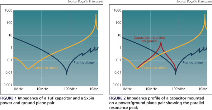
For example, the impedance of a capacitor alone—including its equivalent series resistance (ESR) and ESL as well as due note of how it is mounted—behaves like a simple RLC circuit. The impedance profile of a plane is more complicated, with spreading inductance and resonance effects. Figure 1 shows examples of two such impedance profiles. When the capacitor is mounted on the power and ground planes, there are complex interactions. Figure 2 shows the simulated impedance of this combination.
The test vehicle

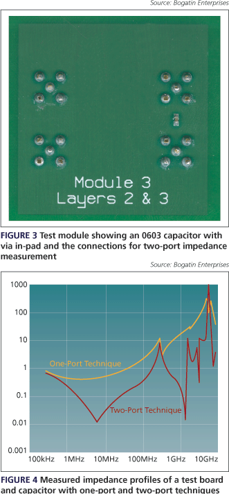
To establish sufficient confidence in the accuracy of the impedance simulation tool, we used a simple six-layer test board. It had 16 different modules with various combinations of plane layers and 0603 decoupling capacitors mounted to its top surface. Figure 3 shows a close-up of one of the modules.
It is easy to measure the impedance as seen by a package pin connected to the power/ground cavity and decoupling capacitors. However, measuring it without fixture artifacts is tricky. In our test vehicle, we used a very powerful two-port method to minimize the effect of the contacts to the planes. Two SMA connectors make contact to the same layer pair in the board, and a two-port VNA is used to measure the two-port S-parameters to these connections.
Normally, a one-port measurement can be used to get the impedance. However, if the calibration is done to the end of the coax cable, the impedance measurement will contain the impedance of the connector to the board. When the impedance you want to measure is in the milliohm range, a connector that might contribute an ohm of impedance at 1GHz is an irritating artifact. It cannot be calibrated or compensated out.
The two-port technique is analogous to the four-point Kelvin technique for measuring very low resistance as a way of eliminating contact resistance artifacts. In the DC technique, one pair of contacts forces a known current while the other pair of contacts measures the voltage generated as this current flows through the resistance of the device-
under-test (DUT). With 1A of forced current, and a measured voltage as low as 1mV, you can easily measure resistances below 1m?.
In a two-port VNA measurement, one port forces a known current through the DUT, while the other measures the voltage across the impedance. The impedance information is in the S21 term.
This technique enables the measurement of milliohms of impedance into the gigahertz range.
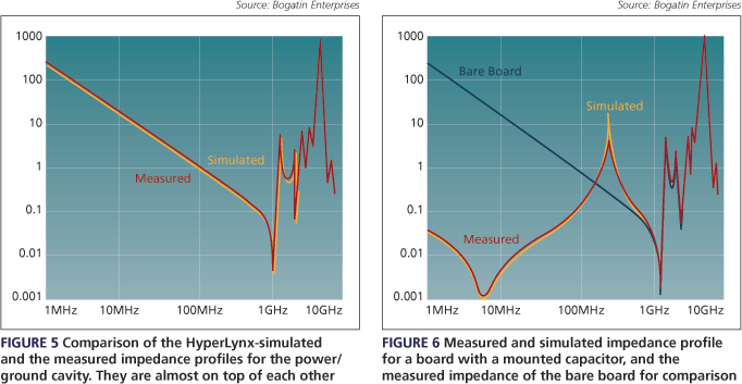
Figure 4 shows an example of the measured impedance of a capacitor mounted to the power and ground planes with a one- and two-port measurement. You must use the two-port VNA technique when measuring the impedance of any element in the PDN, otherwise connector artifacts will dominate the output and the simulation will be inaccurate.
Comparison of simulation and measurement
The aphorism ‘garbage in, garbage out’ was invented to describe simulations. The quality of a simulation can never be better than the quality of the input information about the material properties and geometries of the structures simulated or the models of the components added.
When simulating a bare board, the lateral dimensions, cavity thickness and depth from the top surface as well as the dielectric constant and dissipation factor of the laminate materials are all important parameters for the simulatedimpedance profile.
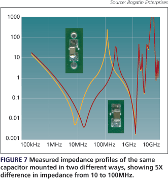
When the correct input parameters are all in place, your ability to predict bare board impedance is excellent, as shown in Figure 5. When a capacitor is added to the board, the agreement between the simulated impedance profile and the measured impedance profile is also very good (Figure 6).

Impact from the mounting structure
You can use these test vehicles and HyperLynx 8.0 to evaluate some recommended design strategies for mounting capacitors to boards. The goal of any PDN design is to reach the lowest possible impedance, especially below 100MHz. Capacitor selection plays a role at low frequency, but has little influence at high frequency. High-frequency impedance is rather about the physical design of the interconnects between the capacitor and the power/ground cavity.
These three factors are important:
- keep surface traces from the capacitor to the vias as short and wide as possible;
- bring the power/ground cavity as close to the surface as possible; and
- use as thin a dielectric as possible between the power and ground planes.
These guidelines will help you to minimize the loop inductance associated with the capacitor to the package pins as well as the impedance at high frequency.

Many vendors offer inductance values for their capacitors as a way of estimating the impedance profile their component may provide. They are completely worthless because the loop inductance of a capacitor depends so strongly on the other interconnects that link it to the power and ground planes. In fact, inductance for the same mounted capacitor can vary by more than an order of magnitude if you change its integration into the board. In the last example, we compare the measured impedance of the same 100nF capacitor, as seen by the two ports of the VNA for different configurations.
Case 1 is a good case: via in pad, power and ground cavity close to the surface and thin dielectric in the cavity. Case 2 is not so good: there are 30mil surface traces from the capacitor pads to the via and the cavity is about 55mil below the surface. Figure 7 shows the measured impedance profiles as seen by the VNA.
The impedance of Case 1 is less than 20% of that for Case 2. This means, if you do the integration right, you could achieve the same target impedance with one-fifth the number of capacitors against Case 2. This could represent a significant cost saving. This comparison emphasizes that there is no magic formula showing how many capacitors to use—it depends so heavily on what mounting inductance you can implement.
You should always follow the design guidelines to minimize the impedance of the PDN as far as possible. But sometimes, that may not be possible because your product faces particular constraints. The power plane may be an odd shape because it shares the same layer as some signals. Or there may be a large clearance hole field due to a BGA. Or the stack up may not allow the power/ground cavity to be near the surface. And so on.
This is why it is essential to explore the design space using an accurate and properly loaded simulation tool if you are to achieve the optimal capacitor selection, number and distribution.
Dr. Eric Bogatin is signal integrity evangelist for Bogatin Enterprises. You can read more of his thoughts on PDNs at www.beTheSignal.com. Chuck Ferry is product marketing manager at Mentor Graphics. You can discover more about HyperLynx 8.0 at www.mentor.com/hyperlynx.