How TI halved the power consumption of Wolverine
Texas Instruments’ MSP430 microcontroller platform has been one of the industry’s leading ultra-low-power architectures for more than a decade. Each generation has been focused on setting new records. The latest, Wolverine, cuts power and energy consumption by more than half.
The next generation Wolverine MCU platform (Figure 1) is codenamed for its aggressive power-saving technology. It achieves a range of new benchmarks for Texas Instruments’ (TI’s) MSP430 architecture that include:
• active power as low as 100 μA/MHz;
• less than 400nA standby with RTC and brownout protection;
• 250X less energy per bit with FRAM; and
• less than 7μs to wake to active from standby.
The overall innovations in Wolverine cut MCU power and energy consumption by half. They have been achieved through the combination of a new 130nm ultra-low-leakage (ULL) process technology, integrated low-power non-volatile memory and enhanced MSP430 DNA with advanced power management and precision low-power analog.
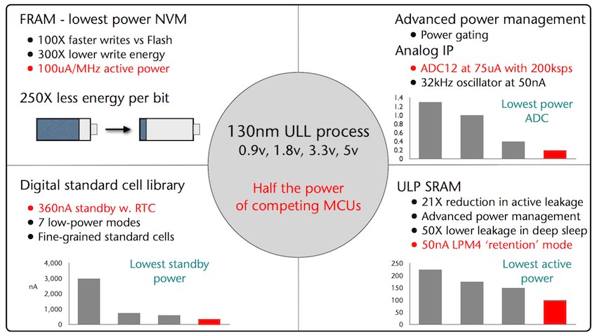
Figure 1
Overview of the Wolverine MCU architecture (Source TI – click image to enlarge)
ULL process technology at 130nm
Given that ultra-low-power devices spend 99.9% of the time in standby mode, leakage current has become key in determining power efficiency at smaller process geometries. The challenge arises from the exponential increase in transistor leakage from ever-shrinking gate lengths and gate oxides.
Leakage current is based on the distance electrons have to travel between nodes and as this distance continues to shrink, the easier it is for electrons to leak across. High-performance microprocessors (MPUs) aimed at 25 or 45nm must use special materials to manage leakage. For MCUs, leakage current becomes a significant consideration from the 180nm CMOS node.
TI has become intimately familiar with leakage current at smaller process nodes through its work on gigahertz smartphone processors and digital signal processors (DSPs) for 65, 45 and 28 nm. Its engineers took everything they learned at those geometries and applied them to Wolverine at 130nm.
Historically, MCU designers targeted innovation in performance and density. Moore’s Law has driven transistor and chip performance. While its pace has slowed over the past decade, process technology has seen a 2X improvement in performance every 18 months for more than 30 years.
For Wolverine, TI has reclaimed the gains of Moore’s Law in the dimension of power instead of performance through circuits designed for power efficiency, optimized for lower leakage current and other characteristics inherent in silicon. Rather than double performance, TI has achieved a 2X improvement in power consumption while maintaining the performance of today’s MSP430 architecture.
The result is at least 10X lower minimum leakage in individual transistors and an overall 15% reduction in active power compared to other 130nm processes (Figure 2).
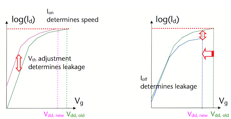
Figure 2
Using a leakage rather than performance-based approach, power losses can be kept low while capitalizing upon the active power benefits from scaling (Source TI – click image to enlarge)
Ultra-low-power foundation
To draw maximum benefit from the 130nm technology, TI completely redesigned its library of design tool kits to focus on power efficiency rather than high performance. These kits – including standard cell libraries, capacitors, analog components and I/O – are based on basic-level transistor configurations that form the underlying building blocks used to design complex MCUs.
The 130nm kits have a large analog component list to enable peripherals like high-precision analog-to-digital converters (ADCs) and internal power management to dramatically lower power.
For example, Wolverine’s module portfolio includes a high-precision 12-bit ADC that can sample 200,000 times per second while consuming only 75μA. Similarly, the real-time clock (RTC) module with calendar and alarm capabilities can run at only 100nA. The 130nm ULL process combined with rich mixed-signal integration makes for the lowest overall system power consumption.
Advanced power management
Efficiency does not apply solely to the power consumption of the CPU. Active current is also dependent upon how the system implements clocking, precision analog peripherals and communications interfaces. The use of advanced power management technology minimizes power consumption under various operating loads.
The Wolverine architecture has an enhanced version of the MSP430 MCU power management module. In addition to seven operating modes, it is capable of advanced power gating and uses a highly responsive adaptive regulator.
Internally, the MCU is divided into multiple power domains to enable the system to dynamically manage each part of the device according to the specific demands of the application.
Total system power consumption is minimized when the amount of time a system spends in standby mode is maximized. However, there is a power cost each time the system switches between standby and active modes. It takes time for the voltage supplied to circuitry to reach the expected level as well as to re-initialize the subsystem or peripheral to become operational again. During this time, the circuitry draws an increasing amount of power without performing any useful work (Figure 3).
Wake-up losses decrease performance, reduce responsiveness and lower power efficiency, especially in systems that frequently switch between active and standby.
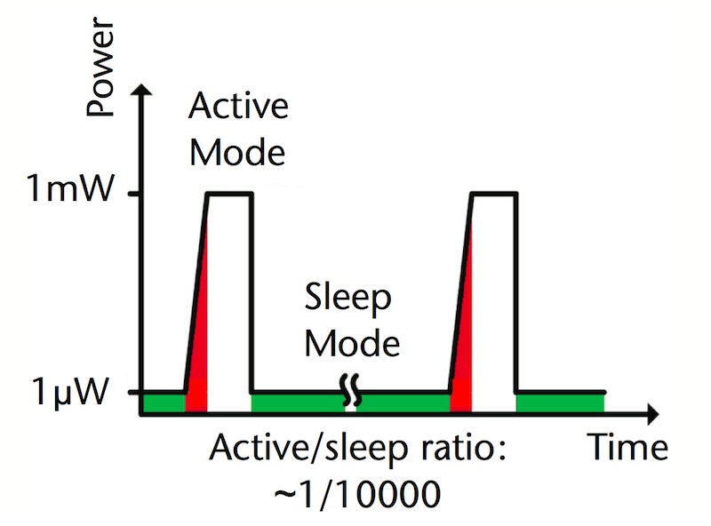
Figure 3
Wake-up losses reduce performance, responsiveness and power efficiency (Source TI – click image to enlarge)
Wolverine takes a different approach to reducing wake-up losses. Traditionally, an entire module or peripheral is shut down when it is not in use. Wolverine instead keeps more of a module or peripheral active in a ‘retention’ mode, using a power-gating controller.
In this mode, modules that are active and requesting a clock are kept fully powered. Modules that are idle and not in use, however, are powered at retention levels. This means that only the logic specific to retaining the state of the module is powered.
Power gating can deliver significant savings without sacrificing performance. Consider a timer in use in standby mode. While it actively requests a clock, the power-gating controller detects the request and maintains it in a fully functional state. However, once the timer function is complete, it is powered down to retention while maintaining the configuration state to minimize power consumption. When the timer is needed again, it is available quickly, minimizing wake losses.
Power gating is transparent to developers, enabling them to take advantage of industry-leading power efficiency without having to manually manage each module or peripheral (Figure 4).
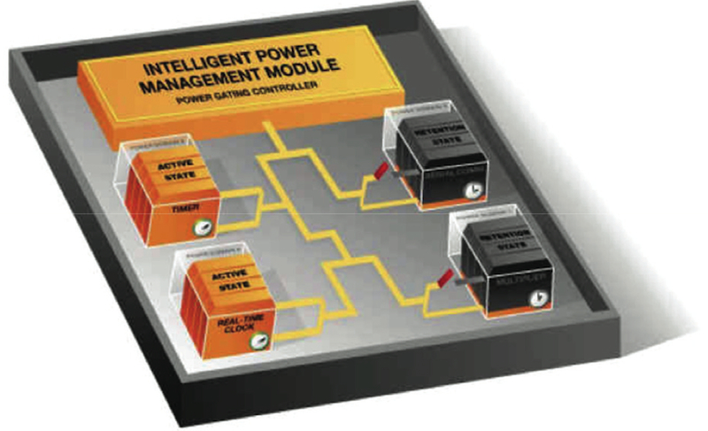
Figure 4
Advanced power-gating in action. Portions not in use are kept at ‘retention state’, so they wake up much faster (Source TI – click image to enlarge)
Another important capability of an ultra-low-power MCU is that it can respond quickly to changing application loads. Substantial power savings can be gained through technology that reduces the power to the main CPU when its full performance is not required.
However, rather than require developers to manually adjust power, the intelligent power management module in Wolverine automatically adapts to changes in application load such as when a high frequency module is powered on (Figure 5).
Figure 5
Wolverine’s intelligent power management module automatically adapts to changes in application load for transparent scaling (Source TI – click image to enlarge)
Specifically, the adaptive low dropout regulator (LDO) that powers the digital core of the MCU responds to changing power requirements by increasing its load as needed (Figure 6). In effect, Wolverine automatically detects the current needs of the application and provides the clock and power as required.
Figure 6
Wolverine automatically detects the current needs of the application, then dynamically adjusts the LDO to match power and clocking needs (Source TI – click image to enlarge)
With high granularity, the LDO can match a wide range of diverse application loads. This approach also eliminates the need for external components (e.g., buffer capacitors) used when switching from low-to-high-load currents. As with power gating, this technology automates power management in a manner that is seamless and transparent to developers.
Ferroelectric random access memory
MCU program code and key system parameters are typically stored in non-volatile memory, most commonly Flash or EEPROM. The slow write time of Flash, combined with its high power and low endurance, prevents its use for data storage. As a consequence, MCUs typically have at least two types of memory: Flash for code; SRAM for data.
To overcome the limitations of Flash, TI integrated another non-volatile memory bit – ferroelectric random access memory (FRAM) – into Wolverine. FRAM is like DRAM except that data is stored in a crystal state, not by charge. As a consequence, it has read/write access and fast cycle times similar to DRAM.
FRAM is also a random access memory where each bit can be read or written individually. In addition, it features a simple, single-step write process. This means no separate erase is required before a write as is the case with Flash.
FRAM is highly efficient compared to Flash memory (Table 1). To write to Flash requires 10–15V and a charge pump. This adds a few milliseconds of charge time. Writing to Flash is also a multi-stage operation during which interrupts must be disabled. This factor complicates block writes to Flash since the system must break up such writes into smaller blocks between which interrupts can be enabled so that no critical signals or events are missed.
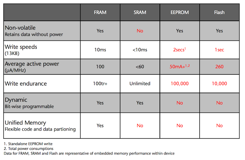
Table 1
Memory type comparison (Source TI – click image to enlarge)
FRAM requires only 1.5V to write. Combined with write times 100X faster than Flash, FRAM’s active write energy is up to 250X lower. System reliability is also maintained without added programming complexity since interrupts can be active during FRAM operations.
Flash has limited endurance (on the order of 100K writes) before its reliability begins to degrade. As a consequence, system parameters are often only saved to Flash when the system is powered down. The effectively unlimited endurance of FRAM (on the order of 1015 writes) enables developers to rethink how they store system parameters.
Specifically, rather than store parameters in SRAM and save them to Flash upon power down, all data can be already stored in non-volatile FRAM, even when it frequently changes. This yields further cost savings since parameters do not need to be actively saved and a capacitor is not required.
System wake-up is also improved. In automotive applications, for example, settings do not need to be restored to the data memory upon power-up since they are already available in the common FRAM space. This also increases the efficiency of highly power-constrained applications, such as those that use energy harvesting. Since no power is required to store and restore data between sleep sessions, applications can operate with smaller energy-harvesting circuitry, thus reducing system complexity and cost.
This is just one example of how FRAM enables developers to rethink their system architecture in ways that increase operating life, reduce system cost and boost reliability. Another key capability of FRAM is its ability to stand as both program and data memory.
In Flash-based systems, the ability to optimize a system based on code and data size is limited to how much Flash and SRAM an MCU has integrated on it. FRAM, with its fast write access and great endurance, can serve as both program and data memory.
The MSP430FR58xx series, the initial Wolverine-based devices, will offer 64 Kbytes of memory and full flexibility in how developers allocate this memory between code and data. This also gives designers the ability to use smaller MCUs with different memory ratios than have previously been available.
In addition, TI has integrated a memory protection unit (MPU) to prevent data operations from accidentally overwriting system code as well as lockable code segments for additional memory protection.
Wolverine-based devices will also have a block of SRAM. This memory is available for applications that truly require the unlimited endurance of SRAM for certain operations. The SRAM block will also help simplify the porting of existing MSP430 MCU designs.
Effective processing efficiency
For ultra-low-power applications, cutting power consumption in half is much more desirable than doubling processor speed. By increasing how quickly the system can go to sleep and wake, developers can fit more processing into the same time and power profile, providing an effective increase in processing speed.
This also gives developers more control over managing power in their designs. Rather than using a smartphone-class MCU for an embedded application, developers can leverage power-efficient devices and scale to the exact level of performance they need.
Wolverine devices will be consistent with existing MSP430 MCU tools and software. Built-in hardware in the silicon and tool chain will enable developers to track energy usage in real-time for accurate power profiling that eliminates guesswork when estimating system power consumption and effective operating life. TI will also provide optimization tools designed to analyze code to assure power efficiency.