Ensuring reliability through design separation
System designs have traditionally achieved reliability through redundancy, even though this inevitably increases component count, logic size, system power and cost. The article describes the design separation feature in Altera software that seeks to address these as well as today’s conflicting needs for low power, small size and high functionality while maintaining high reliability and information assurance.
FPGAs are a ubiquitous part of today’s processing landscape. Their use has extended from their long-established role as glue logic interfaces to the very heart of the advanced information-processing systems used by core Internet routers and high-performance computing systems. What
remains common throughout this evolution is the drive to integrate more functionality in less space while decreasing power and cost.
High-reliability system design—as well as other system design areas such as information assurance, avionics and industrial safety systems—sets similar requirements for reduced system size, power and cost. Traditionally, high-
reliability systems designs have approached reliability through redundancy. The drawback with redundancy, however, is increased component count, logic size, system power and cost.
Altera has developed a strategy that addresses the conflicting needs for low power, small size and high functionality while maintaining the high reliability and information assurance these applications require. The design separation feature in its Quartus II design software and Cyclone III LS FPGAs gives designers an easy way of executing high-reliability redundant designs using single-chip FPGA-based architectures.
Life-cycles and reliability
The concept of reliability engineering has been driven by the U.S. Department of Defense (DoD) since its first studies into the availability of Army and Navy materiel during World War II. For example, the mean time to failure (MTBF) of a bomber was found to be less than 20 hours, while the cost to repeatedly repair the bomber would eventually reach more than ten times the original purchase price. Subsequently, the total life-cycle cost has become a critical metric for system specification and design.
High-assurance cryptographic systems have historically followed a similar path. Failures in a cryptographic system affect the total life cycle in such fundamental terms as security for military systems and commerce for financial systems. Given this context, high-assurance cryptographic systems have similar design and analysis requirements to high-reliability systems.
In each case, the designer’s goal is to shrink the PCB size and reduce the number of components needed for a particular application. This has been the trend in the electronics industry for decades, most recently in system-on-chip (SoC) ASICs and today progressing to SoC FPGAs. Developing SoC ASICs consolidated external digital logic into a single device. This paradigm progressed successfully until the cost and schedules of ASIC development exceeded market money and time budgets. With ASIC costs having grown so much, system designers are increasingly turning to FPGAs where performance and logic densities enable logic consolidation onto a reprogrammable chip.
However, while the growth in SoC designs has been steady for many years, the design and complexity of FPGAs have until now prevented the integration of redundant designs. Many system and security analysts deemed the analysis necessary to verify separate and independent datapaths too difficult.
By working with certification authorities, Altera has simplified complex FPGA device analysis and ensured separate and independent datapaths. By providing users with FPGA tools and data flows that have this analysis in mind from the start, we enable designers to consolidate fail-safe logic designs into a single FPGA fabric. This allows them to meet development budgets and also the requirements of high-reliability and high-assurance applications.
Information-assurance applications
Information-assurance equipment must provide a high level of trust in the design and implementation of the cryptographic equipment. Guaranteeing a complex system design is trustworthy requires robust design standards and system analysis, and several security-design standards and evaluation bodies exist. While explaining the design requirements and evaluation criteria used by each of these bodies exceeds the scope of this article, an overview of their evolution and complexity is shown in Figure 1.
Source: Altera
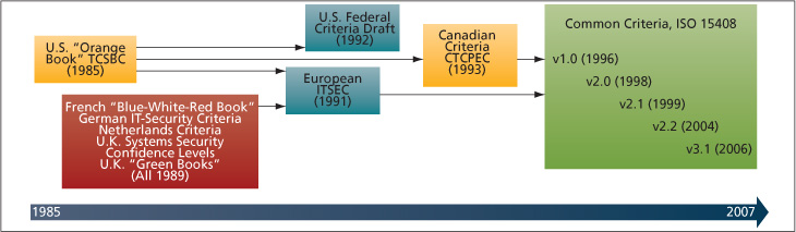
FIGURE 1 Evolution of security criteria design and analysis
IT systems have the greatest influence on information assurance. With an ever-increasing number of infrastructure-control systems, and with corporate and personal information accessible via the Internet, they are increasingly relied on to protect sensitive information and systems from hackers and criminals.
To provide information assurance on the Internet, a user must not only inspect data for viruses, but also protect sensitive information by using security and encryption technologies such as IPsec and HTTPS. While the HTTPS cryptographic algorithm is typically implemented in software running on a computer platform, IPsec and virtual private network (VPN) encryption applications usually require higher performance and rely more heavily on hardware. Network IT equipment must be evaluated at all appropriate levels to ensure trust in the overall system.
This trust must be proven by hardware analysis of each IT component, ensuring that information-assurance levels meet the security requirements of either the Common Criteria or Federal Information Processing Standard (FIPS) 140-2 or 140-3. As shown in Table 1, this analysis is complex and can greatly extend the design cycle.
Source: Altera
|
# |
Section |
Security Level 1 |
Security Level 2 |
Security Level 3 |
Security Level 4 |
|
1 |
Cryptographic module specification |
Specification of cryptographic module, cryptographic boundary, approved algorithms, and approved modes of operation Description of cryptographic module, including all hardware, software, and firmware components Statement of module security policy |
|||
|
2 |
Cryptographic module ports and interfaces |
Required and optional interfaces Specification of all interfaces and of all input and output datapaths |
Data ports for unprotected critical security parameters logically separated from other data ports |
||
|
3 |
Roles, services, and authentication |
Logical separation of required and optional roles and services |
Role-based or identity-based operator authentication |
Identity-based operator authentication |
|
|
4 |
Finite state model |
Specification of finite state model Required states and optional states State transition diagram and specification of state transitions |
|||
|
5 |
Physical security |
Production-grade equipment |
Locks or tamper evidence |
Tamper detection and response for covers and doors |
Tamper detection and response envelope EFP and EFT |
|
6 |
Operational environment |
Single operator Executable code Approved integrity technique |
Referenced PPs evaluated at EAL2 with specified discretionary access control mechanisms and auditing |
Referenced PPs plus trusted path evaluated at EAL3 plus security policy modeling |
Referenced PPs plus trusted path evaluated at EAL4 |
|
7 |
Cryptographic key management |
Key management mechanisms: random number and key generation, key establishment, key distribution, key entry/output, key storage, and key zeroization |
|||
|
Secret and private keys established using manual methods may be entered or output in plaintext form. |
Secret and private keys established using manual methods shall be entered or output encrypted or with split knowledge procedures. |
||||
|
8 |
EMI/EMC |
7 CFR FCC Part 15, Subpart B, Class A (Business use), Applicable PCC requirements (for radio) |
7 CFR FCC Part 15, Subpart B, Class B (Home use) |
||
|
9 |
Self tests |
Power-up tests: cryptographic algorithm tests, software/firmware integrity tests, critical functions tests, conditional tests |
Statistical RNG tests callable on demand |
Statistical RNG tests performed at power-up |
|
|
10 |
Design assurance |
Configuration management (CM)Secure installation and generation Design and policy correspondence Guidance documents |
CM system Secure distribution Functional specification |
High-level language implementation |
Formal model Detailed explanations (informal proofs)Preconditions and post conditions |
|
– |
Mitigation of other attacks |
Specification of mitigation of attacks for which no testable requirements currently are available |
|||
TABLE 1 FIPS 140-2 security requirements
Commercial cryptography
The financial industry today drives the development of commercial cryptography and cryptographic equipment. Its need for information assurance has become ever more pervasive, as its use of technology has grown from inter- and intra-bank electronic data interchange (EDI) transactions, to public automatic teller machines (ATMs), to high-performance cryptographic applications driving electronic commerce.
Like the military, commercial electronic commerce needs commonly accepted standards for the design and evaluation of cryptographic hardware. The financial industry’s need for cryptographic interoperability has been a key differentiator in this market. Commerce extends beyond national boundaries and therefore so must the cryptographic equipment it uses. A major complication in this landscape is the classification of cryptography as a regulated technology under the International Traffic in Arms Regulations (ITAR). High-performance electronic-commerce cryptographic equipment is developed mainly by large server manufacturers that can invest in the expertise and long design cycles necessary to create FIPS 140-2-certified modules.
High-reliability applications
Industrial applications also take advantage of the design separation and independence available from FPGAs. For example, increasing numbers of embedded control units (ECUs) are used in automobiles with increasing complexity and functionality. ECU designers must maintain reliability while reducing size and cost. An ability to separate redundant logic within a single FPGA allows them to reduce the number of system components while maintaining fault isolation.
Design separation
Information-assurance and high-reliability applications currently require at least two chips to ensure the logic remains separate and functions independently. This ensures that a fault detected in one device does not affect the remainder of the design. In cases where design separation is critical—such as financial applications, where data must be encrypted—data must not be able to leak from one portion of the design to another in the event of an inadvertent path being created by a fault. In cases where high reliability is critical—such as industrial systems where entire manufacturing lines may be shut down if one piece of equipment fails—redundant circuits continue to control the system in the event of a main circuit failing, ensuring little to no downtime.
Source: Altera
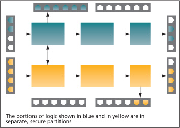
FIGURE 1 Design separation for high reliability and information assurance
The design separation feature in the Quartus II design software allows designers to maintain the separation of critical functions within a single FPGA. This separation is created using Altera’s LogicLock feature. This allows designers to allocate design partitions to a specific section of the device. When the design separation flow is enabled, as shown in Figure 2, each secure partition has an automatic fence (or ‘Keep out’ region) associated with it. In this way, no other logic can be placed in the proximity, creating one level of increased fault tolerance.
However, to ensure true separation, the routing also must be separated. Therefore, all routing is restricted to the LogicLock area of the design partition. This means that the fence region does not contain logic and does not allow routing to enter or exit the fence, ensuring the region’s physical isolation from any other function in the device. Routing interfaces can then be created using interface LogicLock regions. These interface LogicLock regions can route signals into or out of separated regions by creating an isolated channel between two separated partitions. This is effectively the same as using two physical devices to ensure separation.
Altera has designed the Cyclone III LS fabric architecture to ensure the separation results in an increased fault tolerance with the minimal fence size, enabling designers to use over 80% of the resources for their design. The design separation flow also enables specific banking rules that ensure the separation created in the fabric for critical design partitions extends to the I/Os. The Cyclone III LS packages also are designed to support such I/O separation.
Single-chip high-assurance design flow
This uses a standard incremental compile design flow (Figure 3) with five additional steps during floorplanning:
- Create design partition assignments for each secure region using incremental compilation and floorplanning. Each secure region must be associated with one partition only, which means the design hierarchy should be organized early in the design process.
- Plan and create an initial floorplan using LogicLock regions for each secure partition. Top-level planning early in the design phase helps prevent and mitigate routing and performance bottlenecks.
- Assign security attributes for each LogicLock region. Locked regions are used for those parts of a design that require design separation and independence.
- Assign routing regions and signals. To ensure each signal path is independent, a secure routing region must be created for every signal entering or leaving a design partition.
- • Assign I/Os. Each secure region with fan-outs to I/O pins cannot share a bank with any other secure region to ensure design separation and isolation.
The design separation feature is fully supported using the Mentor Graphics ModelSim verification environment, allowing designers to achieve high system reliability through logical redundancy. ModelSim allows designers to verify the functional equivalence of redundant logic on a single Cyclone III LS FPGA.
Conclusion
Requirements for high-reliability and information-assurance systems have many similarities. Both systems require design separation and independence, as each system requires redundancy to ensure proper design operation in the event of hardware faults. Traditionally, the implementation of redundancy increases system size, weight, power and costs because this redundancy is implemented at the board level. To reduce these factors, low-power FPGA processes can be used with a high-assurance design flow to meet stringent NSA Fail Safe Design Assurance requirements.
By ensuring design separation and independence, redundant logic can be transferred from the board level to a single FPGA as part of a SoC design approach. Combining low-power, high-logic density and design-separation features allows developers of high-reliability, high-assurance cryptographic and industrial systems to minimize design development and schedule risk by using reprogrammable logic, and to improve productivity by using a proven incremental-compile design flow.
Further information
- Cyclone III FPGAs—Security, www.altera.com/products/devices/cyclone3/overview/security/cy3-security.html
- Partitioning FPGA Designs for Redundancy and Information Security, webcast,
- www.altera.com/education/webcasts/all/wc-2009-partitioning-fpga-redundancy.html
- AN 567: Quartus II Design Separation Flow, www.altera.com/literature/an/an567.pdf
- Protecting the FPGA Design From Common Threats, www.altera.com/literature/wp/wp-01111-anti-tamper.pdf
Altera
101 Innovation Drive
San Jose,
CA 95134
USA
T: 1 408 544 7000
W: www.altera.com
