DFM will change the industry’s business models
Introduction
As semiconductor manufacturing moves into the sub-100nm realm, the need for increased cooperation and communication between design and manufacturing becomes more apparent. Manufacturing is becoming increasingly complex, and many of the principles that have guided design and manufacturing no longer apply. Some of the major changes occurring in wafer manufacturing include:
- The industry is moving to subwavelength lithography. Beginning at 180nm, minimum features on the wafer were smaller than the wavelength of light used to produce them. As the difference between the printed feature size and the wavelength used to produce it increases, traditional rules of optics no longer apply, and extensive use of resolution enhancement techniques (RETs) is necessary.
- Traditional scaling no longer applies. After 90nm, each node brings a new set of problems. In the past, moving to the next node followed traditional scaling, whereby the same basic device structure was reduced in size, and the same basic materials and structures remained. This is no longer the case.
- Each new node uses new manufacturing processes and materials. The switch from traditional aluminum/silicon dioxide interconnects to copper/low-k structures was only the beginning. As we move to smaller nodes, even lower-k dielectrics with porous structures will emerge. High-k dielectrics with metal gates will appear, as will completely different transistor structures.
- Process windows are getting tighter. The allowable variability of each process step is dramatically decreased, imposing morestringent controls on both manufacturing and design.
- There were about 50 separate design rules at the 180nm node; this increased to roughly 100 rules at 130nm and skyrocketed to more than 1,200 rules at 90nm. Going to more-advanced nodes, design rules will continue to proliferate.
- Mask costs are increasing. At 90nm, a full set of masks for an aggressive design may cost $1m and take weeks to produce. This makes the costs of a design ‘re-spin’ excessive.
- Available market windows for new products are getting shorter. Time-to-yield and time-to-volume production are thus becoming more important.
‘Design for manufacturability’ has been part of semiconductor design for some time. However, as leading-edge manufacturing moves through the 90nm node to 65nm, it takes on new meaning. Because of the issues cited above, it is no longer acceptable to generate a new design and mask set, run it through the fab to see how it will work, and then generate numerous design modifications, each with its own new mask set, until a workable design is obtained. The new goal is ‘right first time’. Incorporate the necessary checks and balances into the design phase to ensure that a new product will produce acceptable results the first time it is replicated.
Achieving this will not be easy. It requires new modes of cooperation between manufacturing and design to ensure that all the complexities of advanced manufacturing are reflected in the design software. Static process models that were adequate up until 130nm must evolve into dynamic models with almost continuous feedback from manufacturing as solutions for yield problems are developed.
DFM will evolve from its present state of checking a design against well-defined rules and adding the necessary RET enhancements to the mask layout. In the future, DFM will include all the necessary analytical capabilities to guarantee that the design will work to specifications when it is manufactured. At present, designs are relatively transportable and can be produced at a variety of fabs using similar processes. In the future, each design will incorporate detailed information about the specific process used in the fab by which it will be manufactured and thus be less transportable. Fabless companies working at the leading edge will have to commit to their manufacturing partner before the initiation of a design; once the details of the specific manufacturing process are reflected in the design, the fabless company will be committed to that partner. Conversely, any change foundries make to the manufacturing process cannot adversely affect customer designs made to the previous process version. Foundries will have to expand relationships well into the design phase.
Achieving sufficient interaction will require the implementation of real-time feedback between manufacturing and design, and continuous improvement of design process models. This will begin at 45nm; by 32nm, almost all process details will have to be communicated to the design staff and reflected in EDA software.While this will produce challenges for integrated device manufacturers (IDMs), it will be increasingly difficult to implement in a fabless/foundry model, in which the foundries’ most valuable IP — full details of the manufacturing process — will have to be made available to the device design team. This will lead to new business models and may strain the fabless/foundry relationship.
EDA vendors will also have to greatly improve their knowledge of manufacturing to develop advanced design tools with embedded DFM capabilities. Traditionally, design and process engineers had vastly different mind-sets, but this has to change. Design engineers must develop a working knowledge of manufacturing process complexities to evaluate the design trade-offs required. The challenge for EDA vendors will be to develop tools that can help device designers understand the manufacturing process and how it determines basic design parameters.
DFM evolution
Established IC computer-aided manufacturing tools, which encompass technical CAD and RETs, can handle design requirements for 130nm and 90nm manufacturing. Below 90nm, the increasing difficulty of successfully producing a given design forces designers to consider manufacturing issues earlier. Figure 1 shows the status of DFM activities and their projected evolution as manufacturing capabilities move toward 32nm production in 2010.
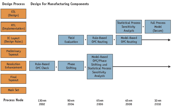
Figure 1. The evolution of DFM
Today, most DFM offerings focus on the generation and verification of RET mask enhancements. At 130nm, the addition of optical proximity correction (OPC) features to masks is sufficient; at 90 nm, more aggressive phase shifting mask (PSM) techniques are being added to OPC. Current generation RET algorithms use fixed rules to create the necessary features. One of the challenges with implementing advanced RET features on mask sets is verifying that the mask, once produced, replicates the desired layout. Accordingly,many DFM products are aimed at RET verification. They simulate the effects the RET features will have on pattern replication and seek to minimize re-design before initial mask generation.
At 90nm, we are seeing the introduction of automated analysis of device layouts to identify areas that may cause potential yield losses. This uses the feedback from the manufacturing analysis of test chips that have been specifically designed to generate data about which types of layout may cause yield problems. This marks the beginning of a use of sophisticated models of process behavior to examine the yield effects of design trade-offs.
At 65nm, the DFM picture becomes more complex. As the mask generations step, rule-based RET evaluation will evolve into a model-based evaluation of the interactions between OPC and PSM enhancements. These models will use feedback from the manufacturing floor to evaluate the effects of lithography process variability on the effectiveness of RET efforts on mask production. The objective is to evaluate the sensitivity of specific mask feature sets to normal variations in wafer fabrication processes. However, to ensure that these model-based RET verification steps produce the desired results, design layout rules will have to expand to include layout restrictions based on OPC implementation rules.
Consequently, at 65nm, the design layout will have to consider not only the massive set of fixed design rules, but also evaluate layouts for potential yield effects and modifications that may be dictated by OPC additions to the mask.
By 45nm, rule-based OPC checks at the layout stage will be replaced by model-based analysis of the effects of various OPC trade-offs on device layout.More importantly, the first design implementation efforts after electrical system design will also have to consider a statistical process model, which evaluates all aspects of the new design against the complex interactions of all process steps. Such a model will go far beyond an analysis of the design’s capability to be replicated accurately in silicon; it will evaluate whether the manufacturing process is capable of achieving the desired device performance to identify the changes needed to ensure device success.
At 32nm, the statistical process model will expand to a full-modelbased simulation of the wafer manufacturing process.Well before the design layout stage, the desired design characteristics will be evaluated against a simulated run through the manufacturing process to determine areas of design weakness. This new model will contain a full and complete characterization of the manufacturing process in sufficient detail to allow the process to be replicated in any advanced 32nm-capable fab. By this time, a given device design will become fab-specific; that is, it will include features refined for the specific manufacturing process, and even specific process tools, as defined in the process model.
As wafer processing moves from 90nm to 32nm, DFM concepts will also evolve. However, during this evolution, designs will gradually become more and more process-focused, so that, by the end of the decade, the most-advanced device designs will incorporate features based on the particular process selected in advance to manufacture the design.When this happens, once a design is completed, it can be manufactured only at the specific fab it was designed for, or one running a duplicate process.
