Clock domain crossing: guidelines for design and verification success
Clock domain crossing (CDC) errors can cause serious design failures. These can be avoided by following a few critical guidelines and using well-established verification techniques. The guidelines include: When passing 1bit between clock domains:
- register the signal in the sending clock domain to remove combinational settling; and
- synchronize the signal into the receiving clock domain. A multi-cycle path (MCP) formulation may be necessary.
When passing multiple control or data signals between clock domains:
- first attempt to combine multiple signals into a 1bitrepresentation in the sending clock domain before synchronizing the signal into the receiving domain; or
- use Multi-Cycle Path (MCP) formulations to pass multiple signals across clock domains; or
- use FIFOs to pass multi-bit buses, either data or control buses; or
- use gray code counters.
Partition the design sub-blocks into completely synchronous one-clock designs.
Use a clock-based naming convention.
Multi-strategy CDC verification:
- run a full structural CDC verification at the RTL level;
- use formal analysis or instrumented simulation to ensure functionality; and
- re-verify that gates (post-synthesis & scan insertion) still adhere to proper CDC design rules.
Clock Domain Crossing (CDC) design errors can cause serious and expensive design failures. These can be avoided by following a few design guidelines and using well-established verification techniques. This paper details some of those methods that enable design teams to avoid problems and verify compliance with good CDC design techniques.
Single bit CDC
Several problems relate to passing a single bit between clock domains. Many of these issues and their potential solutions are documented in [3].
Before passing any signal between clock domains, fi rst register the signal in the sending clock domain. If a signal is allowed to pass through combinational logic before it is passed into a receiving clock domain, it may experience combinational settling. A signal that experiences combinational settling in fact creates more edges that can be sampled in the receiving clock domain and therefore more chances that a changing signal will be sampled while changing and cause metastability. By registering a signal before allowing it to pass a CDC boundary, you remove the multiple combinational settling edges and limit potential transitions to one edge per sending clock cycle, thereby reducing the potential for generating metastable signals.
MCP formulation and usage
Another important technique used to pass signals between clock domains employs a multi-cycle path (MCP) formulation.
For signals that traverse between clock domains, the effects of metastability must be localized and controlled at the crossing. This is most often done by creating data-control pairs, in which the data piece is a single bit or multiple bits, and the control piece is typically a single bit passed through a synchronizing pulse generator to load the data piece into the receiving clock domain. The data and control signals are sent simultaneously. This causes the data to be stable for multiple cycles in the receiving clock domain while the control signal is synchronized into a load pulse in the receiving clock domain.
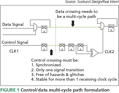 The control and loading logic is constructed in such a way that the data transfer is forced to be a multiple cycle transfer controlled by a synchronized enable or control signal. This structure is shown in Figure 1. Data is passed from the sending domain into the receiving clock domain without synchronization, but the loading of the data into the receiving register is controlled by a synchronized ‘control’ or ‘enable’ signal after synchronization and edge detection.
The MCP description in the diagram refers to the fact that the datapath is held stable for multiple cycles until the enable/ control pulse is passed through multiple clk2 synchronization stages. Since the data signals are not sampled until the enable/ control signal arrives multiple cycles later, there is no danger of the data signals being sampled while changing and therefore no danger that the data signals might become metastable when ultimately sampled into the receiving clock domain.
Use FIFOs on grouped CDC signals
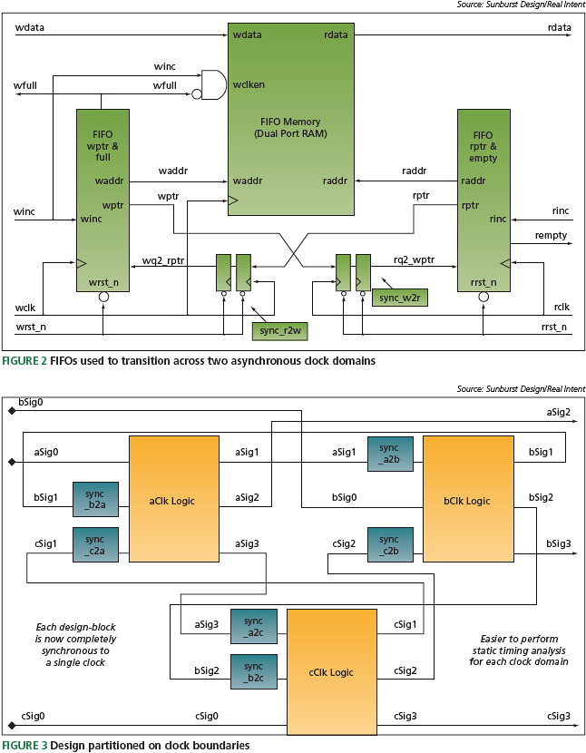
Another popular way of transmitting data or multiple control signals reliably across the CDC boundary is based on the use of FIFOs. A good FIFO design technique is described in [2] and a block diagram is shown in Figure 2.
The FIFO controls the flow of the multi-bit control or data signals while transitioning from the sending clock to the receiving clock. The multi-bit signals are placed into a shared memory buffer (typically, a dual port RAM) from the sending clock domain and removed from the shared memory buffer in the receiving clock domain.
Use gray codes counters
Several applications require counter values to be passed between clock domains, such as FIFOs. Trying to pass binary count values over CDC boundaries is as problematic as passing multi-bit signals between clock domains. The easiest way to pass count values between clock domains is to use gray code counters. These counters only change one bit at a time so they do not suffer from multi-bit synchronization problems.
In many applications, such as FIFO designs, you do not need to reliably sample every gray count value and missed gray count values do not pose a problem. In such cases, using a double fl ip-fl op synchronizer on each bit of the counter is good enough without the need to acknowledge receipt of each gray count value.
Design partitioning
There are two approaches to addressing potential CDC problems: (1) using techniques that actively avoid the issue; and (2) verification against qualifi ed CDC rules. Both should be used to ensure an error-free design. In this respect, engineers can adhere to the following design-partitioning guidelines:
Guideline: Allow only one clock per module.
Reason: Static timing analysis (STA) and the creation of synthesis scripts are much easier on single-clock modules or groups of single-clock modules.
Guideline: Partition the design blocks into one-clock modules.
Reason: The timing verification of completely synchronous sub-blocks can be easily verifi ed using STA tools. Partitioning the design blocks into multiple one-clock domain sub-blocks turns a large and complicated timing analysis target into a set of completely synchronous, oneclock designs.
Guideline: Create synchronizer modules for signals passing from a different domain into a new clock domain. Still make sure to allow only one clock per synchronizer module.
Reason: It is a given that any signal passing from one clock domain to another clock domain is going to have setup and hold time problems. Isolate these problems at the fi rst stage input fl ip-fl ops of the synchronizers and keep them away from timing analysis required on design blocks. Also, gate-level simulations can be more easily confi gured to ignore setup and hold time violations at the fi rst stage of each synchronizer.
Clock naming conventions
Guideline: Use a clock-naming convention to identify the clock source of every signal in a design.
Reason: A naming convention helps each team member identify the clock domain for every signal in a design and also makes grouping of signals for timing analysis easier, using regular expression ‘wild-carding’ from within a synthesis script.
Several clock-naming conventions are available. One proven example uses a prefi x character to identify the various asynchronous clock domains (i.e. ‘uClk’ for the microprocessor clock, ‘vClk’ for the video clock, ‘dClk’ for the display clock, etc.). Each signal is then synchronized to one of the clock domains in the design and each signal-name is labeled with a prefi x character to identify the clock domain used to generate that signal. For example, any signal generated by uClk is labeled with a u-prefi x (e.g., uaddr, udata, uwrite, etc).
An engineer can thus easily identify the clock-domain source of any signal in the design and either use the signals directly or pass them through proper synchronization so that they can be used within a new clock domain. The exact naming convention is not important, but it is important that everyone agrees to adhere to the one that is chosen.
Multi-strategy CDC verification
The above guidelines, combined with careful design review, will improve CDC design quality. But there is no substitute for complete and exhaustive verification. To verify the structure and functionality of the design a multi-step process is required.
Run the full structural template for CDC verification at the RTL level
In the fi rst step, the tool traverses the entire design looking for CDCs. Signals that are synchronized are classifi ed as control, while unsynchronized signals are classifi ed as data. Control/data pairs are matched up, and the connectivity is verifi ed to be correct for passing unsynchronized data using a synchronized enable signal. Multi-bit control signals must exhibit gray behavior, and the structural analysis detects these for later analysis. Also, FIFO structures are identifi ed and verifi ed when they are present.
This is a good way to detect simple errors cheaply. Common problems caught this way include the lack of proper control/data formulation, missing or duplicated synchronizers, combinatorial logic past the sending register, and the reconvergence of control signals.
Formal analysis to ensure functionality
Some CDC errors may remain undetected after the structural template analysis because the process lacks the precision of formal analysis. To verify functionality, CDC tools use some combination of formal analysis, and dynamic analysis. Formal analysis can be applied to ensure that the register in the receiving domain is an MCP with respect to the clock in the sending domain (e.g., the receiving register must not load on the fi rst clock from the receiving domain). Formal analysis can be used to prove the gray-code behavior of multi-bit control signals, and also to verify that glitch-related errors are absent from CDC interfaces.
Dynamic CDC analysis
Dynamic analysis is a technique that makes use of the design’s existing simulation testbench. In this way, the whole simulation regression can be run on the design with one major change: the signal transitions at a CDC boundary randomly incorporate the effects of metastability (e.g., glitch capture, loss of correlation, transfer delay, etc.). If the design still gives the correct results from the testbench under these harsh conditions, the CDC is defi – nitely valid.
Post-synthesis CDC verification
It is well understood that the post synthesis design may differ from that of the RTL [4]. Synthesis and other transformations such as scan insertion can cause CDC errors. Therefore, CDC verification must be run on the fi nal netlist to guarantee that the design is CDC-clean before fabrication. Post-synthesis analysis entails new tool requirements around handling library cells and memories. It also creates capacity and memory challenges, especially on large designs. Even factoring in these challenges, the cost of a CDC error at this late stage is so high that gatelevel CDC verification is a requirement.
Summary
Following simple guidelines related to CDC design and using specialized automated CDC verification can help to avoid problems and increase your chances of rapid multiclock design success.
One other fi nal point worth making is that when evaluating commercial CDC tools, pay attention to the volume and value of the reports. A tool that generates an inordinate volume of messages and/or where results require lengthy analysis can obscure real problems and offer little or no gain. Choose a tool that generates the important information in a concise and manageable report.
References
[1] William J. Dally and John W. Poulton, Digital Systems Engineering, Cambridge University Press, 1998
[2] Clifford E. Cummings, “Simulation and Synthesis Techniques for Asynchronous FIFO Design,” SNUG 2002 – www.sunburst-design.com/papers/CummingsSNUG2002SJ_ FIFO1.pdf
[3] Clifford E. Cummings, “Synthesis and Scripting Techniques for Designing Multi-Asynchronous Clock Designs,” SNUG 2001 – www.sunburst-design.com/papers/ CummingsSNUG2001SJ_AsyncClk.pdf
[4] Don Mills & Clifford E. Cummings, “RTL Coding Styles That Yield Simulation and Synthesis Mismatches” SNUG 1999 – www.sunburst-design.com/papers/ CummingsSNUG1999SJ_SynthMismatch.pdf
[5] Prakash Narain, Real Intent, Inc. (white paper), “Clock Domain Crossing Demystifi ed: The Second Generation Solution for CDC verification,” February 2008 – www. realintent.com
Sunburst Design
14314 SW Allen Blvd.
PMB 501 Suite 210
Beaverton OR 97005
USA
T: +1 503 641 8446
W:www.sunburst-design.com
Real Intent
505 North Mathilda Avenue
Sunnyvale CA 94085
USA
T: +1 408 830 0700
W: www.realintent.com
