A top-level verification methodology including power supply and signal check using mixed-signal simulation
The ‘state-of-the-art’ solution for wireless transceiver RF ICs is single chip CMOS, integrating digital, analog, and RF blocks on a single chip. The architectures involved require new and challenging approaches to verification. To understand these, we first need to look back at the history of the transceiver architectures used for wireless mobile phone implementations during the last decade.
Initially, transceivers consisted of many single components. The RF-core and building blocks were realized in bipolar technology since these transistors had the required speed and properties needed for wireless applications. The digital blocks were designed separately on CMOS. But in the next advance, more digital functionality was integrated.
A shift to combined Bipolar/CMOS technologies (BiCMOS) then took place. The verification was done separately for each single block or component, according to the block specification defined by the concept engineer. This involved simulations based on SPICE and/or HDL netlists.
Over the last five years, it has become clear that this approach does not address the increasing complexity of new transceiver architectures. Simulation time has been increasing dramatically from hours to days or even weeks. On the other hand, the cost of technologies with smaller gate lengths has increased. A methodology is needed that avoid re-designs and delivers ‘first-time right’ silicon. In this paper we will describe such an approach, covering multiple supply domain levels and interconnectivity checks as key aspects of the verification challenge.
The verification challenge
The verification solution we were looking for was driven by the nature of our wireless communications products — specifically, our goal of delivering the first 0.13um CMOS single chip radio transceiver including baseband. The transceiver is aimed at the market for GSM/GPRS dual, triple and quad-band mobile phones and data modems.
A top-level verification of the baseband and transceiver chip seemed too difficult to undertake as the first step. Setting up an overall top-level verification of a transceiver alone is challenging because it includes the RF, analog and digital parts.
The transceiver chip includes a fully integrated RF VCO and supports the full quad-band (GSM850/900/1800/1900MHz). Low-noise balanced amplifiers (LNAs) for the four bands are integrated on the single chip, as well as a synthesizer for ultra fast locking and a digital modulator. The different blocks have different power supply domains: digital blocks have a 1.5V supply; analog blocks often have a 2.5V supply. Blocks are switched on and off during operation to save battery power.
The main challenges are summarized in Figure 1, a very basic block level diagram of the current generation of this RF-transceiver using a polar modulation architecture.
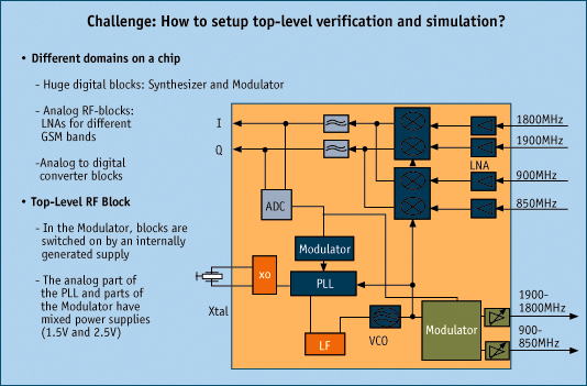
Figure 1. Top-level verification challenges illustrated with relation to the architecture of a single chip polar modulator transceiver
Top-level verification methodology
The following boundary conditions determined the verification methodology.
- Different domains such as digital, analog, and RF on a single chip.
- HDL (VHDL and Verilog) behavioral models are used to describe huge digital blocks.
- VHDL, VHDL-AMS and SPICE are used for analog and RF-blocks.
- Signal inputs from the baseband block are stored in a VHDL-model.
- There is the presence of different power supply and signal domains (1.5V and 2.5V).
Methods such as the formal verification approach used in digital designs are not applicable to designs that include analog and RF blocks. The top-level design is put together in a schematic. Connecting all the sub-blocks from the top-level is very error-prone.
- Wrong supplies can be connected.
- Signals can be twisted.
- Internal generated power supplies can be dynamically switched on or off, too early or too late.
- A basic architectural problem from the interaction of analog/mixed signal circuit blocks with digital blocks can show up in the complete design.
The choice for verification is top-level mixed-signal simulation. For pure digital blocks, a script-based flow is used. VHDL models are the source and RTL netlists are generated. To build analog and mixed signal blocks, the Cadence Database and Schematic Entry tool is used. The RTL netlists are transferred into the Cadence database as behavioral views. The blocks could have different
representations such as ‘schematic’, ‘behavior view A’ or ‘behavior view B’. The different behavior views contain the model description at different levels of accuracy. The Cadence Hierarchy Editor is used to choose which of the respective views is most relevant to each simulation task that will be undertaken. A respective netlist for the Mentor Graphics ADVanceMS mixed-signal simulator is then generated and mixed-signal simulation is performed.
To detect problems such as wrongly connected power supplies or blocks being switched on or off too early/or too late, a new approach to setting up behavioral models is required. In Standard Libraries and written HDL models, power supplies are not taken into account.
Basic concept
Let us take a look at the kind of simple inverter cell typically provided in Standard Libraries (Figure 2). As long as the inverter is simulated with the schematic view (Figure 2, left), the power supplies are taken into account. But if the Verilog/VHDL behavioral view model is used (Figure 2, right), a mismatch arises. The inverter model will work independently of the value of the VDD supply. Therefore, we need to add the power supply ports to the model and include a check algorithm that detects the value of the power supply and input signals.
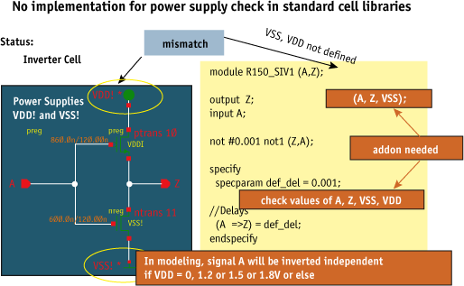
Figure 2. Concept for basic power supply check
Implementation
Most often, two different standard cell types are available at the same time in CMOS technologies for different power supply domains: one for 1.5V, offering high speed; the other for 2.5V with less speed performance but higher breakdown voltages. Of course, a 2.5V cell is logically working correctly when operated on a 1.5V supply, but its maximum operating frequency is reduced. Nevertheless both cell types must be used either for level shifting or simply because there is no other supply voltage available locally at a sub-block.
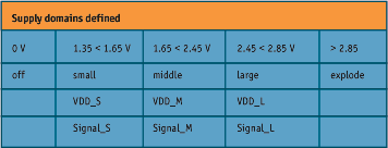
Figure 3. Distinguishing different supply domains
For power supply and signal ranges, different value regimes are defined (Figure 3, p25) for all relevant and available transistor types. They are implemented as enumeration data types. So, 0V is defined as ‘off’. By contrast, a signal or supply above 2.85V will destroy all device types and is defined as ‘explode’. Between those values, different voltage ranges are allowed depending on the transistor type used.
Different scenarios need to be taken into account when the different cell types are used in a design and somehow interact. In the designs blocks, 1.5V, 2.5V and mixed supply domains exist. The check mechanism shown below only works if the block is described in HDL. For 1.5V blocks, three scenarios are checked (Figure 4).
In case one, the supply voltage is smaller than 1.35V but does not equal 0 and the input signal is between 1.35 and 1.65V. This leads to an undefined (X) output signal.
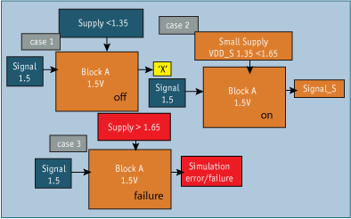
Figure 4. Cases for power supply and signal check for 1.5V blocks
In case two, the input voltage and input signal are in the expected range and a signal with a property ‘Signal_S’ is the output.
In case three, the supply voltage is above 1.65V and the input signal is in the expected range. During simulation, an error occurs and an error message pops up saying that on a specific instance the power supply VDD exceeds the allowed maximum.
In Figure 5, the different cases for different input signals with the correct power supply are listed.
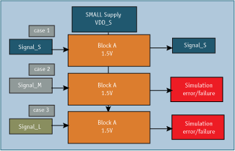
Figure 5. Cases for correct supply but different input signal ranges
In the case where the input signal is in the range of 1.35 to 1.65V, labeled as ‘Signal_S’, the combination of ‘VDD_S’ and ‘Signal_S’ leads to an output signal of type ‘Signal_S’.
In case two, the power supply is still in the expected range of ‘VDD_S’ but the input signal is in the range between 1.65 to 2.45V, labeled as ‘Signal_M’. This input signal is not in the allowed range and during simulation an error occurs.
In the third case, where the input signal is in the range between 2.45 to 2.85V (which is too high), the same behavior as in case two is seen. During simulation an error occurs and the instance where the problem occurred is listed.
So far all possible scenarios for 1.5V blocks have been discussed. For 2.5V blocks, all combinations also have to be taken into account. The method is the same as described above for 1.5V blocks.
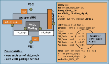
Figure 6. VHDL wrapper including power supply and signal check
To achieve this approach, behavioral models have to be adopted. So that we can still run simulations with and without the power supply and signal check, the original HDL models are left untouched. A VHDL code wrapper is generated with the respective checks, and all ports have user-defined enumeration types and additional ports for the power supply. The original HDL code is instantiated in the VHDL wrapper code. An example of the implementation is given in Figure 6 (p27).
The power supplies are defined as VHDL real types. To distinguish the different signal domains — ‘Signal_S’, ‘Signal_M’, and ‘Signal_L’ — user-defined enumeration VHDL types called ‘pcheck_ulogic’ are defined in respective packages. They are subtypes of ‘std_ulogic’. In the VHDL wrapper, the voltage ranges given in Figure 3 are defined (Figure 6, right). Each wrapper model gets the information about its intended power supply. The checks are performed in the architecture of the VHDL wrapper.
One benefit here is that the wrapper can be applied at any digital/model-based design level. There is no need to wrap each single standard cell by itself; in the complex netlist of a digital sub-hierarchy this netlist/behavioral description can be wrapped as a whole if all cells within this design hierarchy are operated from the same supply. The overall simulation time is therefore not greatly influenced because the wrapper functions do not need to be triggered for any internal occurring simulation event.
To setup the simulation, the Cadence Virtuoso, Hierarchy Editor and Analog Design Environment toolsets are used. The partitioning of the top-level design is done in the Hierarchy Editor. Partitioning entails selecting which block is simulated on a SPICE level and which is simulated on a behavioral model basis. The configuration also allows the user to define whether the power supply and signal check is performed or not.
For the mixed-signal simulation, the ADVanceMS mixed-signal simulator from Mentor Graphics is used. If an error occurs, an error message pops up during simulation where the supply or signal is not in the expected range. Using this method, several errors, such as twisted signals or wrongly connected power supplies, were detected before tape-out.
Conclusions
We have outlined a top-level verification method that is applicable to CMOS wireless products. This method makes it possible to check the correctness of power supply and signal domains in the top-level design. The verification methodology is based on developing simulation and VHDL wrapper models where the checks are performed. It helped us to find design errors and avoid re-designs as a result of wrongly connected signals and power supplies. The approach brought us one step further towards our goal of ‘first-time right’ silicon.
References
- Mayer, T., Neurauter, B., Springer, A., “A fully integrated, automatically adjusted CMOS RF phase modulator for cellular applications,” Proc. Radio and Wireless Symposium, IEEE, pp. 567- 570, 17-19 Jan. 2006
Infineon Technologies
Development Center MŸnchen
Am Campeon 1-12
D – 85579 Neubiberg
Germany
Tel: +49 89 234 0
www.infineon.com


