Toward usable and scalable DFT for 3D IC design
 Wu Yang is the technical project management director for Tessent design-for-test products at Siemens EDA.
 As 3D IC grows in use, there has been increasing discussion around the design-for-test (DFT) requirements it sets for both 2.5D lateral and 3D stack designs. Siemens EDA has taken proactive steps to develop DFT solutions that enable customers to meet the challenges involved.
Figure 1 shows a 2.5D layout. It has multiple ICs packaged side-by-side on a common interposer.
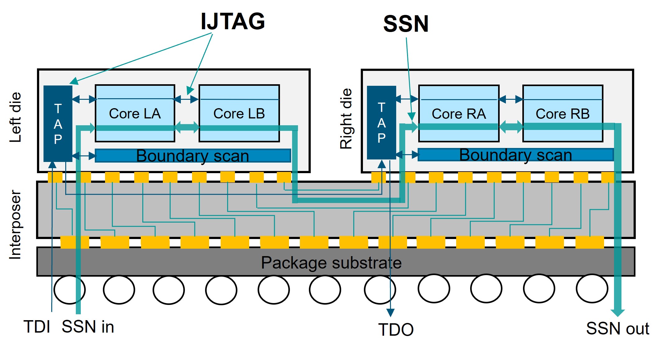
Figure 1. DFT architecture for 2.5D ICs (Siemens EDA – click to enlarge)
A 2.5D layout has more relaxed test accessibility than a 3D stack (Figure 2) where dies are stacked on top of each other.
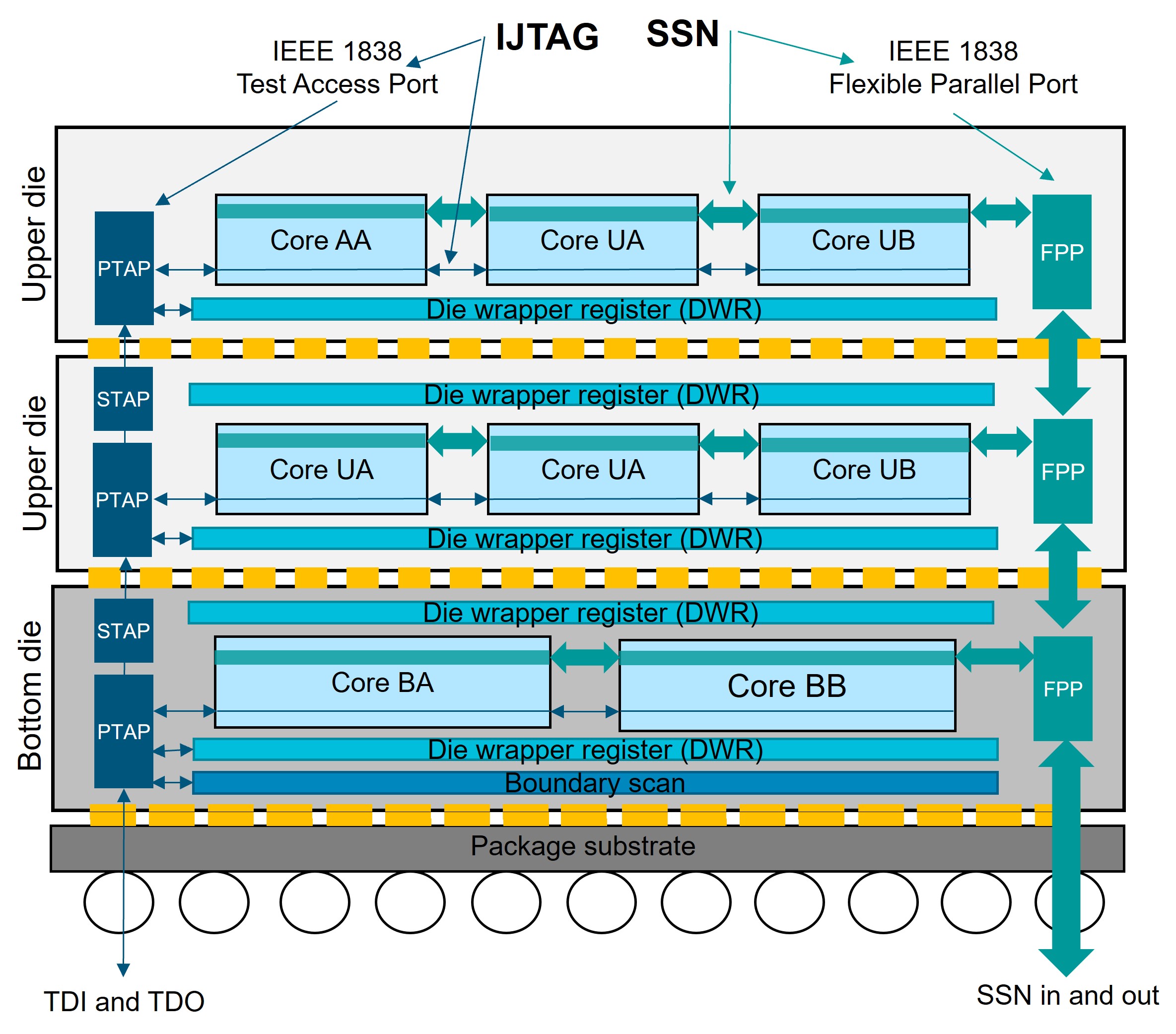
Figure 2. DFT architecture for 3D stack ICs (Siemens EDA – click to enlarge)
The IEEE 1838 standard defines hardware and test access protocols for every die in a 3D stack. These include a mandatory serial port using primary (PTAP) and secondary (STAP) TAP to help inter-die communication; die wrap registers (DWR) to handle die-to-die test; and a flexible parallel port (FPP) for transporting scan data in and out of the dies in the stack.
DFT for 2.5D architectures requires a package-level IEEE 1149.1 compliant test access port (TAP), package-level boundary scan; and IJTAG support. It also needs a way to transport the scan data in/out of the dies in the package.
Though there are some different DFT requirements for 2.5D and 3D designs, they also share a good number in common. These similarities include:
- Dies need to be tested on wafer where few die PADs are available for probing by testers yet test quality has to be maintained.
- When dies are packaged, they need to be tested inside the package with either very limited pins in a 2.5D design or by going through the base die of the 3D stack. Test quality must address issues around low pin and low test cost.
- Dies need to have standard interfaces for inter-die communication and die-to-die connections. These need to be fully tested.
- Complex DFT structures at the sub-die, die, and package levels require the use of a network and a language to manage the DFT operation.
- Robust diagnosis is required at the sub-die, die, and package levels.
The Siemens EDA IC test solution addresses these requirements.
Complying with standards while addressing 2.5D and 3D differences
For a 3D stack to be IEEE 1838 compatible, standard-compliant PTAP/STAP, DWR, and FPP are inserted and modeled with ICL/PDL. In the Siemens solution, the FPP is natively supported by the Tessent Streaming Scan Network (SSN) to deliver packetized streaming data to the dies inside the package.
The dies stacked on top of base dies do not usually have boundary scan; only the base die has boundary scan on the substrate side. All the inserted DFT logic is connected over an IEEE 1687-compatible IJTAG network for automated test operation.
A 2.5D design could allow the TDI to come in and the TDO to come out of the package with different TAPs. This flexibility allows regular IEEE 1149.1 TAP to be implemented on each die and daisy-chained so that it is package-level IEEE 1149.1-compliant. Each die can have boundary scan so that die-to-die test pattern generation can be automated using boundary scan description language (BSDL) for each die.
The package-level BSDL can be extracted to facilitate board-level testing. The DFT operation is handled through the IJTAG network using the same language as that of the 3D stack. If there are external memories (e.g., an HBM2 stack), the PHY uses the IEEE 1500 protocol which can be integrated with the IJTAG network to retarget HBM test patterns to the package level.
Scalability and test economics
Designs are today implemented hierarchically to manage complexity, and so is DFT. The move toward 3D IC adds new sources of complexity such as very limited chip pins and identical die handling. Hierarchical DFT is scalable to 2.5D and 3D stack designs where test pattern generation is done at the sub-die or die level and easily retargeted to the package level.
Using Tessent SSN for FPP resolves these challenges by enabling the simultaneous test of any number of cores or dies with few chip-level pins. The platform has multiple features, such as the use of broadcasting to reduce test time and test data volume either at die or package level (e.g., the user can design a flexible number of SSN bus bits for FPP to address low-pin test).
A 2.5D design may have more DFT pin accessibility so that an SSN bus can be flexibly implemented to come out to the package through a different die (Figure 2).
Automation
The IJTAG network connects all the DFT IPs, and also automates the test setup and DFT network management. Each component on the network is modeled in ICL/PDL so that test patterns at sub-die and die level can be retargeted to the package level. Tessent SSN is a plug-and-play solution handling scan data automatically for compression and automatic test pattern generation (ATPG) to generate low-cost patterns.
DWRs are needed for 3D IC die test at the wafer level where few of the pins are likely to have been wrapped for ATPG. These pins (e.g., TAP pins or SSN pins) can be probed at wafer level and are designed with sacrificial PADs that can be discarded during stacking.
For DWR insertion (Figure 3), automation is done by tracing from the I/O of the die to inside the die to find appropriate registers for building up the DWR chain. The registers may consist of wrapped chains around blocks inside the die, die top-level registers, and boundary scan cells if they are present in the die.
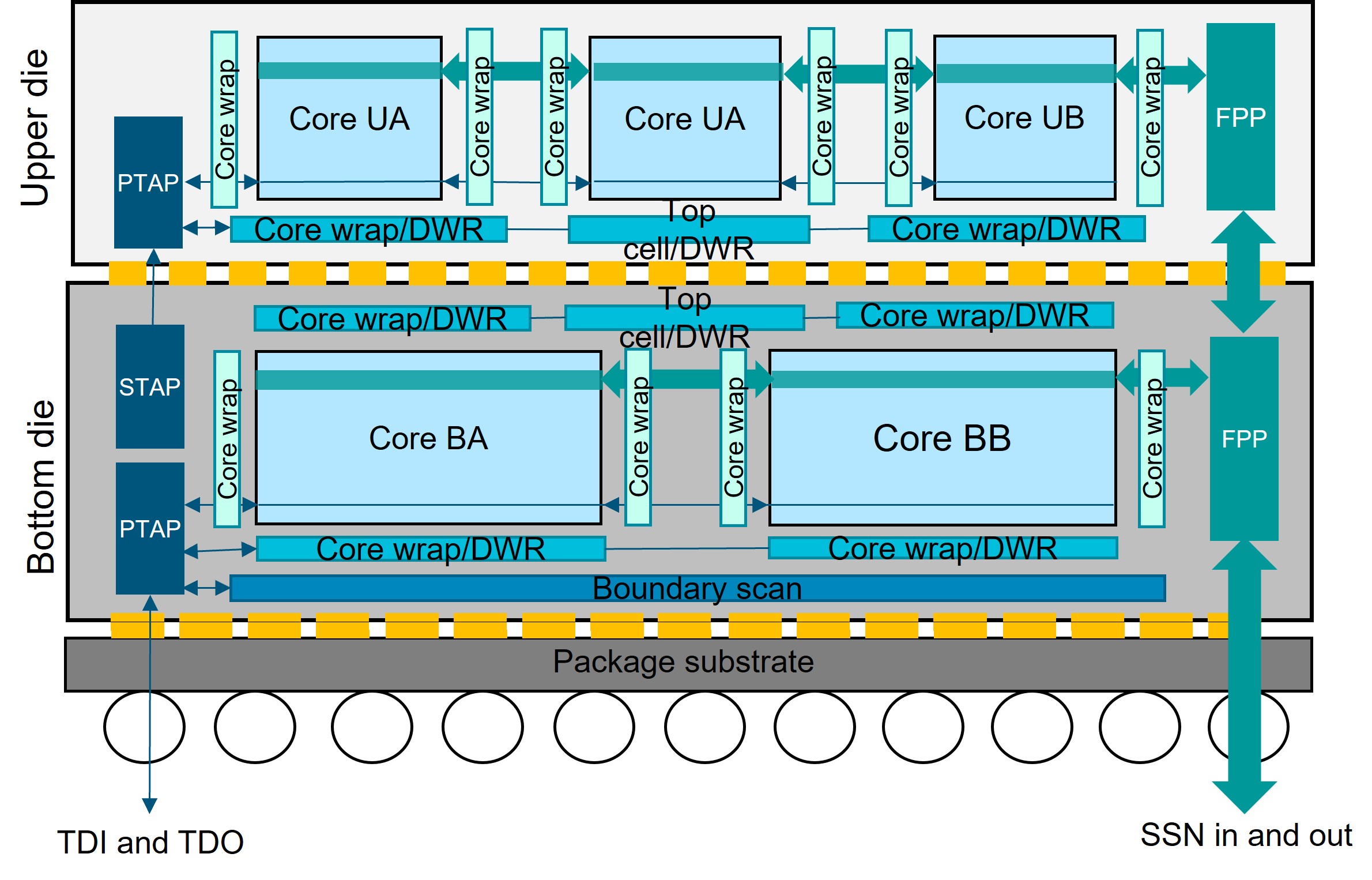
Figure 3. Die wrapper register (DWR) insertion (Siemens EDA – click to enlarge)
The package-level design netlist, with the greybox view of each die wrapped by DWR chains, is used to do die-to-die ATPG with reduced demands on computation resources.
Robust diagnosis and silicon debug
When failures are seen at the package level, the failure data are reverse-mapped to the die or sub-die level to run the same diagnosis as that in a regular hierarchical DFT flow. The die-to-die diagnosis is performed with the package level netlist containing die greyboxes.
While the range of technology for 3D IC test is growing, some tasks remain challenging:
- Die-to-die lane redundancy design and repair where a lane fails. This will can greatly improve the yield of a packaged 3D IC product. This usually requires I/O BIST on each die so that failed lane information can be passed to an analysis engine similar to that of memory BIST BIRA and activate the repair.
- Support for heterogeneous dies in the package where different DFT solutions from multiple vendors are implemented on dies, particularly those at with different technology nodes.
Nevertheless, the fundamental 3D IC DFT technologies are in place, They are available, and they are proven. They include hierarchical DFT, an IJTAG network, SSN, and other recent innovations that comply with the 3D test standards and strategies. The development of automated solutions continues with contributions from players from across the DFT ecosystem.