The simulation and design of software-defined radios
The paper discusses the simulation, design, and test of software-defined radios (SDRs), initially using a legacy 16QAM waveform, followed by a new SDR waveform -orthogonal frequency division multiple access (OFDMA). The SDR system’s error vector magnitude (EVM) is first analyzed and its performance is compared with the legacy waveform results. The implementation also includes the RF transmitter, receiver and channel models, and shows their contributions to overall system response. The presence of in-band and out-of-band co-channel interference at various RF frequencies and power levels and its effect on system performance is also evaluated using the different waveforms. The waveforms are loaded into a Xilinx FPGA and the signals are read into an Agilent logic analyzer or oscilloscope for system-level testing. Simulation and test instrumentation are combined to test the hardware, along with the complete RF system simulation model, to create a software-defined instrument for one-box testing of an SDR with real signals being processed through it.
Introduction
The many definitions of a software-defined radio (SDR) include:
- designs in which the hardware is reconfigurable or reusable for many different software-defined waveforms;
- designs where the baseband may be implemented with FPGAs, ASICs, or DSPs for signal processing to allow reconfiguration of the radio for different waveforms;
- designs where new signal formats featuring waveforms such as orthogonal frequency division multiple access (OFDMA) can be quickly implemented and tested with existing hardware to ensure that they meet specification;
- and designs that improve interoperability by porting waveforms and/or waveform software.
There are significant challenges to designing and testing the physical layer of SDRs. It can be challenging or even impractical to exhaustively test waveform compatibility with hardware test. It may also be hard to accurately replicate field scenarios in the lab through baseband and RF simulations. There is increasing interest in using commercial-off-the-shelf (COTS) waveforms for SDR applications. This can present difficulties in modifying these complex waveforms to match the custom waveform specification requirements of the customer.
SDRs also present a challenge for testing because custom equipment may be required to create and analyze custom proprietary waveforms. In addition to being time and cost prohibitive, custom test solutions often have limited flexibility.
A new design-to-test methodology allows existing baseband hardware waveforms to be captured and used directly to design the SDR system with EDA software. Design simulations can then be used to quickly and efficiently evaluate compatibility with new waveforms before they are implemented with baseband hardware. RF system compatibility to COTS waveforms, such as Mobile WiMAX OFDMA, can allow engineers to run ‘what-if ’simulation and evaluation scenarios. RF interferers or jammers can be introduced in the simulations to evaluate, compare, and contrast the SDR’s susceptibility to various field scenarios prior to field deployment. Additionally, the simulation used for the SDR design can be leveraged directly in instrumentation as a custom application to create software- defined instruments (SDIs) for the testing of SDRs.
Case study: transmitter and receiver design
This study first uses a 16QAM(quadrature amplitude modulation) legacy waveform that has been implemented in FPGA hardware. The FPGA’s output waveform is captured by a logic analyzer and read into Agilent’s Advanced Design System (ADS) EDA software as a simulation signal source (N.B., as an alternative to using the actual FPGA hardware, the same HDL code can be co-simulated and used as the stimulus to the IF section).
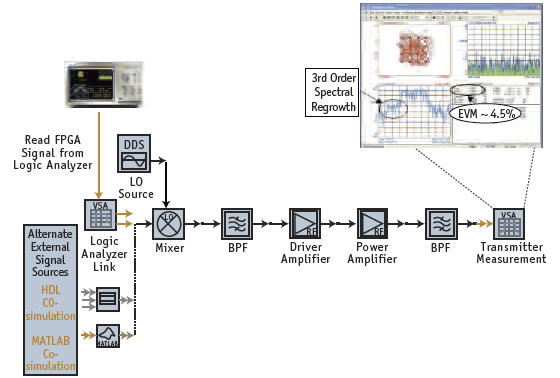 Figure 1. Simulation results for the SDR RF transmitter
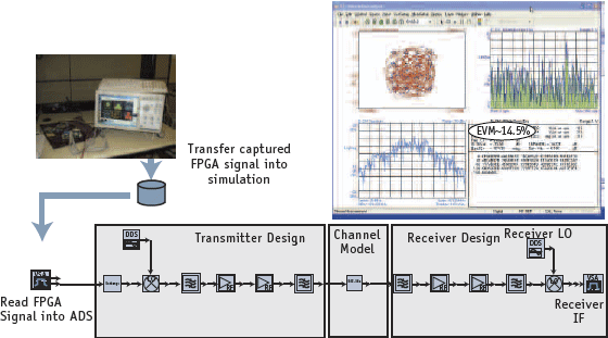
Figure 2. Simulation Results of SDR RF Transmitter and Receiver, with Channel Model
Thus, the RF sections of the radio can be designed using the output of the actual baseband hardware, and baseband algorithm performance can be evaluated in the presence of simulated RF effects. Figure 1 shows the SDR RF transmitter design using the FPGA hardware as a simulation signal source. The transmitter is implemented using RF behavioral blocks such as mixers, filters, and amplifiers where parameters such as gain, compression point, and third-order intercept point can be specified. If circuit level designs or measured results for the blocks are available, they can also be incorporated into the simulation to improve the fidelity of the model. The Vector Spectrum Analyzer (VSA) simulation measurement element is connected to the transmitter output and the simulation results are shown on the top right of Figure 1.
This design example shows the spectral re-growth resulting from gain compression distortion. Also, note that both baseband and RF impairments are included in this simulation because the simulation signal source is, in fact, the captured FPGA signal. The simulated error vector magnitude (EVM) result at the transmitter output is approximately 4.5 % as a result of these impairments.
An RF propagation channel model and receiver are then added to complete the design. The VSA simulation results after the receive chain are shown on the top right of Figure 2. Here, the simulated EVM result at the receiver output has degraded to approximately 14.5% (approximately 10% higher than at the transmitter output in Figure 1) because of channel model and receiver impairments. Clearly the physical RF channel model – which includes effects such as multipath, doppler and physical environmental factors – has a significant impact on system performance.
We will now show how the existing radio’s physical layer RF performance can be evaluated with a new COTS OFDMA Mobile WiMAX waveform.
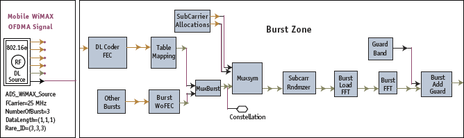 Figure 3. OFDMA Mobile WiMAX baseband coding blocks
Implementing an 802.16e WiMAX waveform
To evaluate the waveform, the FPGA board is initially replaced by a simulated MobileWiMAX signal source (Figure 3). This MobileWiMAX signal source is a hierarchical source, with the lowest level comprised of C++ baseband algorithm blocks, which are designed to functionally represent the baseband coding based upon the 802.16eWiMAX specification. The figure shows a small segment of the coding. These pre-configured baseband codec blocks can help minimize the need to manually code appropriate algorithms.
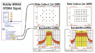 Figure 4. Configurable Mobile WiMAX source parameters
The top-levelWiMAX signal source parameters are configurable and can be easily modified to create many different variants of the OFDMA downlink waveform. As an example, Figure 4 shows simulation sources reconfigured from 10MHz bandwidth using 16QAM to a 20MHz nonstandard bandwidth using 64QAM.
Simulating both baseband and RF in one EDA simulation environment allows for system-level trade-offs, such as evaluation of the effects of baseband bit width, power amplifier nonlinearities, and local oscillator phase noise. It also allows baseband algorithm performance to be evaluated in a ‘real world’ signal propagation environment by including the RF propagation and channel impairments mentioned previously. Although not explicitly discussed in this article, an evaluation could be done to simulate the encoding/decoding baseband algorithms for a multiple input-multiple-output (MIMO) antenna configuration in the presence of a simulated RF multipath and propagation environment. Baseband algorithms written in C/C++, m-code, or HDL that has been written for an FPGA implementation may also be co-simulated and evaluated with the RF designs and RF channel models.
Evaluating interference effects
Here, the system performance is evaluated through a simulated field scenario. An RF interference signal is injected into the signal path at the receiver input and the susceptibility of both the uncoded 16QAM waveform and the coded COTS OFDMAWiMAX waveform are evaluated and compared in its presence (Figure 5).
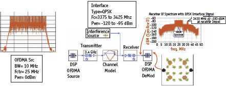 Figure 5. Simulated field scenario: QPSK interference on OFDMA system
A generic filtered quadrature phase-shift keying (QPSK) interference source is created with approximately 1MHz of bandwidth. The main signal is centered at 3400MHz and the interference is initially centered at 3410MHz. The two signals are combined and applied to the receiver input and the plot on the upper right of Figure 5 shows the resulting spectrum at the receiver IF.
Sweeping the QPSK interference frequency from 3375MHz to 3425MHz offers an interesting comparison between the legacy 16QAM waveform and the OFDMA waveform(Figure 6). Unlike the 16QAM signal, the interference has little effect on the OFDMA waveform EVM until it is within the 10MHz OFDMA signal bandwidth. At 3390MHz the QPSK interferer is within the system bandwidth of 30MHz, but the EVM is not affected, and does not degrade until it is within the OFDMA signal bandwidth (3395-3405MHz). By contrast, EVM for the legacy 16QAM waveforms is more sensitive to interference and system performance is degraded over a much wider range of interference frequencies (approximately 3382-3418MHz).
The QPSK interference signal level is then swept from -120dBm to -95dBm with the interference frequency well within the OFDMA signal bandwidth (10MHz). Note that the OFDMA signal is affected at much lower interference levels (~-108dBm for a 1% change) than the 16QAM waveform (~-100dBm for the same change). TheWiMAX waveform still has a significantly better EVM than the uncoded 16QAM waveform, even at higher levels of interference.
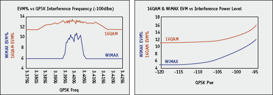 Figure 6. Simulated field scenario interferer results with swept interference frequency (left) and swept interference power (right)
The OFDMA waveform demonstrates an advantage over the uncoded 16QAM waveform in reduced sensitivity to the QPSK interferer, particularly outside the OFDMA signal bandwidth.
Implementing the OFDMA waveform
To implement the OFDMA waveform with FPGA hardware, HDL may be hand-written or generated with EDA tools.
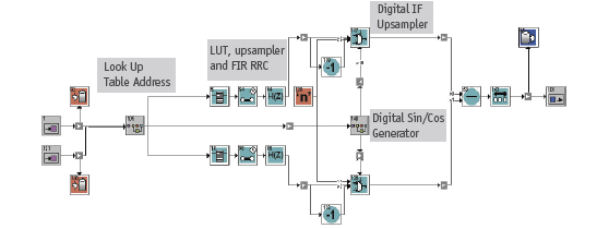 Figure 7. SystemVue IQ modulator with ADS WiMAX IQ data
Agilent’s SystemVue HDS3 capability, developed by Steepest Ascent, is then used to generate VHDL for the in-phase/quadrature (I/Q) modulator directly fromthe schematic shown in Figure 7. This design uses ADS narrowbandWiMAX I/Q waveforms which are stored in ROM. These waveforms are filtered then upsampled to a digital-IF. The resulting VHDL is then co-simulated as shown in Figure 8 to verify performance with the RF transmitter, channelmodel, and receiver. The HDL co-simulation is on the left side of Figure 8 and the VSA systemsimulation results are on the right.
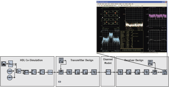 Figure 1. HDL co-simulation with RF transmitter, channel model, and receiver
After verifying the narrowband WiMAX HDL functionality with the RF transmitter and receiver, the HDL is implemented in FPGA for hardware testing with SDIs as discussed in the next section.
Testing SDRs with SDIs
Testing SDRs for waveform compatibility can present a challenge when using COTS test equipment. COTS products may offer commercially available waveform signal generation and analysis, but custom/proprietary waveforms or variants of a commercially available waveform (e.g., modified MobileWiMAX OFDMA) may require custom equipment.
Numerous articles describe the benefits of combining EDA and test equipment solutions, including scenarios that run the EDA simulation software directly inside instrumentation to create SDIs. Leveraging the flexibility of SDIs may be particularly useful for testing SDRs by creating a software-defined library of waveforms to test compatibility. Flexible simulations enable the creation and analysis of custom or proprietary waveforms, and the creation of modified versions of commercially available waveforms (such as a modified MobileWiMAX signal).
Furthermore, field scenarios may be simulated inside the test instrumentation to test hardware in a lab environment before field deployment. The simulation of an RF QPSK interferer inside a logic analyzer to test algorithms implemented with FPGA hardware is, as discussed above, one example.
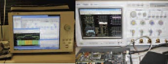 Figure 9. Software defined instrument testing of SDR with FPGA hardware
Figure 9 shows two examples of SDIs configured with ADS as custom application examples. The legacy 16QAM waveform from the FPGA hardware is being generated on the left, with the simulated QPSK interferer being introduced with EDA software inside a logic analyzer to evaluate RF interference effects on the FPGA waveform. The righthand side shows a narrowbandWiMAX FPGA implementation being tested with an Infiniium Oscilloscope that also has EDA software installed in it.
Summary
This article presented a new methodology for SDR design and test.Waveforms from baseband hardware can be captured and used directly to design the SDRs with EDA software. Simulation can be used to quickly and efficiently evaluate compatibility with new waveforms before actually implementing new waveforms with baseband hardware. RF system compatibility to COTS waveforms, such as MobileWiMAX OFDMA, can be evaluated with simulation to evaluate ‘what-if ’ scenarios.
RF interferers can be introduced in simulation to evaluate, compare, and contrast the system’s susceptibility to various field scenarios using EDA simulation before field deployment. Additionally, the susceptibility of an uncoded 16QAM waveform to RF interferers can be compared and contrasted to a coded COTS WiMAX OFDMA waveform. Lastly, EDA can be leveraged directly in instruments to create software-defined instruments for SDR testing.
Acknowledgements
The authors would like to acknowledge Steepest Ascent Ltd for their contributions to the FPGA implementation and Frank Ditore of Agilent Technologies for his contributions to the SystemVue HDL modeling. WiMAX is a trademark of the WiMAX Forum.
Agilent Technologies
5301 Stevens Creek Blvd
Santa Clara
CA 95051
USA
T: 1 800 829 4444
W: www.agilent.com