Implementing an intelligent solar tracking control system on an FPGA
Given present-day demands for environmentally friendly, renewable energy sources, solar energy is becoming increasingly attractive. However, while solar energy is free, non-polluting and, in practical terms, inexhaustible, there remain significant inefficiencies in capturing it. For example, solar panels are traditionally fixed and in this configuration cannot capture the maximum amount of sunlight during changing weather and seasons. This article describes an FPGA implementation of a solar tracking control system that improves the efficiency of solar panels by allowing them to follow the movement of the sun and maintain an optimal position perpendicular to it.
Solar tracking control system design
A high-performance solar tracking system uses two motors as the drive source, conducting an approximate hemispheroidal 3-D rotation on the solar array within a certain amount of space. This rotation allows the system to track the sun in real time to efficiently perform photoelectric conversion and production. The two drive motors are decoupled (i.e., the rotation angle of one motor does not influence that of the other motor), reducing control problems. Additionally, the tracker does not have the problems common to two-axis mechanical mechanisms (i.e., that one motor has to bear the weight of the other motor). This implementation minimizes power consumption during operation and increases both efficiency and the total amount of electricity generated.
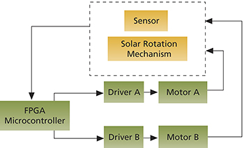
Figure 1. Solar tracking control block diagram. Source: Yuan Ze University
The application uses Altera’s Nios II configurable embedded processor to perform solar tracking. The design combines the embedded processor with a two-axis motor tracking controller, memory and I/O into a single Altera Cyclone II EP2C20F484C7 FPGA (Figure 1). This integration accelerates development while maintaining design flexibility, reduces the circuit board cost via a single-chip solution, and simplifies product testing. The design includes three modes:
- Balance positioning—A tilt switch is used for balance positioning to set the four boundaries of the platform and prevent the solar panels from hitting the mechanism platform and damaging it or the motor.
- Automatic mode—In this mode, the system receives sunlight onto the cadmium sulphide (CdS) photovoltaic cells and the CdS acts as the main solar tracking sensor. The sensor feeds information back to the FPGA controller through an analog-to-digital (A/D) device. The Nios II is the main control core and adjusts the two-axis motor so that the platform is in the location for optimal energy capture and generation.
- Manual mode—If the system has a fault or needs to be maintained, it can be switched to manual mode to be checked or repaired.
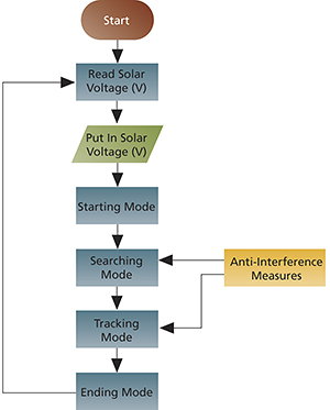
Figure 2. Tracking control flow chart. Source: Yuan Ze University
The logic flow design is implemented with the Nios II processor control circuit. Figure 2 shows the tracking control flow chart. The system starts when the tracking control circuit’s power supply switch is turned on. The tracking control circuit performs system tracking, energy saving and system protection, as well as system control and external anti-interference measures. Sources of external interference include environmental effects such as wind, sand, rain, snow, hail and salt erosion damage.
Design architecture
As shown in Figure 3, the Nios II is the control center and integrates the two-axis control chip. The system determines what data is fed back to the FPGA using a light sensor. It conducts the tracking control rule operation to calculate the angle required by the motor and adjusts the motor’s current angle. It also moves the solar panel to achieve optimal power.
For the hardware design, a balance sensor sets the system’s zero point, and a tracking sensor determines the orientation of the solar light source. The signals fed back by the sensor form the basis of the controller input. The control design outputs the signals to control the two-axis step motor and the solar tracking control system.
Balance sensor
The initial reset balance uses a tilt switch. The mechanism includes four switches (east, west, south and north) that are powered on when horizontal balance is achieved during initial system reset.
Tracking Sensor
The tracking sensor is composed of four similar CdS sensors—located at east, west, south and north—to detect the light source intensity in the four orientations. The CdS sensor forms a 45° angle with the light source. At the CdS sensor positions, brackets isolate the light from other orientations for wide-angle search and quickly determine the sun’s position. The sensors are divided into two groups, east/west and north/south. In the east/west group, for example, the CdS sensors compare the intensity of received light in the east and west.
When they detect differences in the intensity of the light source, the system collects this data and determines which sensor received more intensive light based on the sensor output voltage value interpreted by the voltage type A/D converter (ADC) and ADC0804 device. The system then drives the step motor toward the orientation of this sensor. If the output values of the two sensors are equal, the output difference is zero and the motor’s drive voltage is zero, which means the system has tracked the current optimal position of the sun.

Figure 3. System architecture. Source: Yuan Ze University
The CdS sensors’ output signals generated by the solar light source are the input signals for the ADC chip’s sixth pin. They are converted into analog signals and 8-bit output signals via pins 11-18. Then the signals are sent to the FPGA.
Design methodology
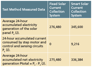
TABLE 1. Collected 24-Hour Solar Energy Radiation (Cloudy). Source: Yuan Ze University
To achieve best performance, solar panels should be perpendicular to sunlight. This section describes how the solar controller is implemented using the Nios II and fuzzy logic.
Solar energy controller production
Although the solar tracking system’s two drive motors can independently rotate without the problem of coupling, they do face nonlinear phenomena at the moment of inertia, a common problem for 3-D rotation mechanisms. Therefore, the motors require a closed loop control. Although nonlinear phenomena exist at the moment of inertia control, the tracking system does not need to rotate very quickly due to the speed of the sun’s movement. Fuzzy control rules can be used to control the motor operation while ensuring the system control mechanism is sufficiently adjustable and has a fast response time.
A hardware control circuit written in VHDL or Verilog loads the control program into the Nios II. The sensor, decoder and other devices form a complete control loop, ensuring the system’s optimal efficiency.
Fuzzy logic controller implementation
The controller design (Figure 4) takes the measured value of the light strength received by the sensor as the feedback and implements control using many rounds of modifications. The CdS sensor’s resistance changes with the light strength. Fuzzy control takes the errors of the two groups in the vertical (south/north) and horizontal (east/west) axes as the inputs.
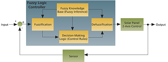
Figure 4. Solar energy fuzzy control system structure. Source: Yuan Ze University
FPGA Design
The system-on-a-programmable-chip (SOPC) design methodology incorporates the hardware system (including processor, memory, peripheral interface circuit and user logic circuit) and software design on a single piece of silicon.
For hardware development, the team used Altera’s Quartus II software for design entry, compilation, place and route, and FPGA programming. LeonardoSpectrum software was used for circuit synthesis and ModelSim was used for system simulation; both tools are from Mentor Graphics.
LeonardoSpectrum was used to compile the HDL programs and generate EDIF netlists, which were then compiled by the Quartus II software. During software design, we used the GNUPro software development tool and software resources such as header files, library, monitors and peripheral drivers to generate and edit application code. We debugged the software using standard debug and profile tools included with GNU, then simulated the hardware running our software using ModelSim’s simulation environment. When we found an error, we were able to modify and regenerate the hardware using Altera’s SOPC Builder design tool. Finally, we downloaded the hardware and software design into the development board and prototyping kit for circuit verification.
Figure 5 shows the system development flow. The system—including the processor, memory interface, peripherals, arbitrator and custom instructions—was specified with SOPC Builder. Here, we could choose either an ARM Cortex M1 or Altera Nios II CPU to embed into the FPGA as VHDL or Verilog HDL.
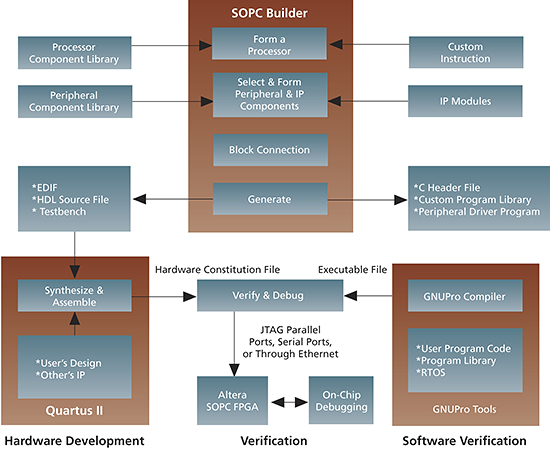
Figure 4. SOPC system development flow. Source: Yuan Ze University
The soft-core Nios II is a 32-bit configurable embedded processor. For peripherals, Altera provides on-chip ROM, on-chip RAM, external memory interfaces (such as SDRAM, SSRAM and DMA controllers), serial I/O (such as UART and Ethernet), parallel I/O (such as an input/output/two-way port, or PCI interface) as well as timers (such as a simple timer, frequency timer and watchdog timer). Altera also provides a PCI 32/33 bridge and Ethernet MAC.
SOPC Builder automatically generated a custom interconnect fabric to connect all system components. We implemented the Nios II processor in a Cyclone II EP2C20F484C7 FPGA on an Altera Development and Education (DE1) board.
Design features
The Nios II processor helped implement the design in the following ways:
- The major difference between this and traditional, single-chip designs is that the circuit included a fuzzy control rule. Traditional devices required external logic circuits to implement a fuzzy controller, increasing the controller design volume and cost. Alternatively, a combined microcontroller (MCU) and FPGA (excluding the Nios II) solution would, self-evidently, be a two-device assembly.
- For complex logic circuits, we can create a design using an FPGA and the Nios II processor. By this method, we can use the C language to write fuzzy algorithms and incorporate them into the Nios II CPU and compile the VHDL code into the FPGA to control the stepper motor. This implementation allows us to process algorithm operations and I/O control in parallel, improve integrated efficiency, and quickly implement and verify our hardware circuits.
System testing
We tested the system both indoors and outdoors. During the outdoor test, we moved the solar platform to the top of a building so we could compare the results between fixed position and smart collection systems. During a 24-hour trial, the smart collection system was required to operate for approximately 30 seconds every hour to maintain proper alignment with the sun. During that period, the solar panel charged for about eight hours; the rest of the time it did not consume power (i.e., there is no standby mode). Comparing the total net electricity generation of the fixed elevation angle control and smart solar tracking control, we found that the smart system was 22% more efficient.
For the indoor test, we used a searchlight as a simulated sunlight source, established a fixed and smart simulated sun running orbit, and used Visual Basic (VB) to transmit the measured voltage to a notebook computer to measure the actual voltage through the RS-232 port. Results showed the voltage of the fixed solar current collection system was less than that of the smart solar current system. Therefore, the smart system was proven to be superior to the fixed system.
Yuan Ze University
135 Yuan-Tung Road
Chung-Li
Taiwan 32003
R.O.C.
T: +886-3-463-8800
W: www.yzu.edu.tw
Altera Corp
101 Innovation Drive
San Jose
CA 95134
USA
T: +1 408 544 7000
W: www.altera.com


