Demystifying analog and mixed-signal ASICs
The article reviews the design assessment process that a company should undertake when developing an analog-centric application-specific integrated circuit (ASIC). The authors argue that a number of myths surround strategies that incorporate a large amount of specialist analog design work, including evaluations related to cost and functionality. In particular, the need for differentiation in today’s fast-expanding analog market is addressed.
To better understand the role and applicability of ASICs, we need to briefly review their origins. The first digital ASICs were built using standard cell libraries consisting of fixed-height, variable-width ‘tiles’ containing digital logic functions. An ability to reuse these blocks saved time and money when designing a custom logic IC.
Analog ICs initially comprised a pair of matched transistors and soon expanded to include rudimentary op-amps, voltage regulators, comparators, timers and more. Analog applications typically require much higher voltages so these ICs also needed their own custom manufacturing processes.
More recently, market demands for smaller size, higher speed and lower power consumption have forced the merger of analog and digital functionality on a single silicon chip. Cells consisting of the basic analog building blocks have been created and added to digital libraries.
These analog cells are usually restricted to the digital fab processes developed for logic devices. Today, most ASIC companies offer some degree of analog functionality as a part of their services. In many cases, analog functions are mimicked with digital design techniques. In others, compromises to the analog functionality must be made to facilitate the use of standard library cells that are designed to yield well in fab processes developed for high speed, high density, low power digital designs. These chips are often referred to as ‘mixed-signal’ or ‘big D-little A’ ASICs, the latter term most specifically referring to a combination of high digital and minimal analog content.
Analog ASICs play a critical role in our lives. Without them, none of the portable electronic devices we use would exist. Imagine a world without cell phones, MP3 players and navigation systems. Building these gadgets with standard products would make them prohibitively expensive and physically impossible to carry in our purses or pockets. Every automobile contains dozens of ASIC chips for functions ranging from climate control to airbag deployment; from suspension control to entertainment systems. ASICs also play important roles in applications for hospital equipment, eMeters, home appliances, hearing aids, and much more.
The analog ASIC market is huge (Figure 1). Researchers at IC Insights estimate that almost 60% of the nearly $37B of analog ICs sold in 2010 were ASICs. Yet very few mixed-signal ASIC design houses fully understand the implications of custom analog design. ASICs requiring a high analog content should be directed to those design houses that specialize in analog circuit design rather than those who simply select IP blocks from a library. Reviewing an ASIC house’s patent portfolio is a quick guide as to the creativity of its engineering team and will serve as a first order measure of its analog expertise.
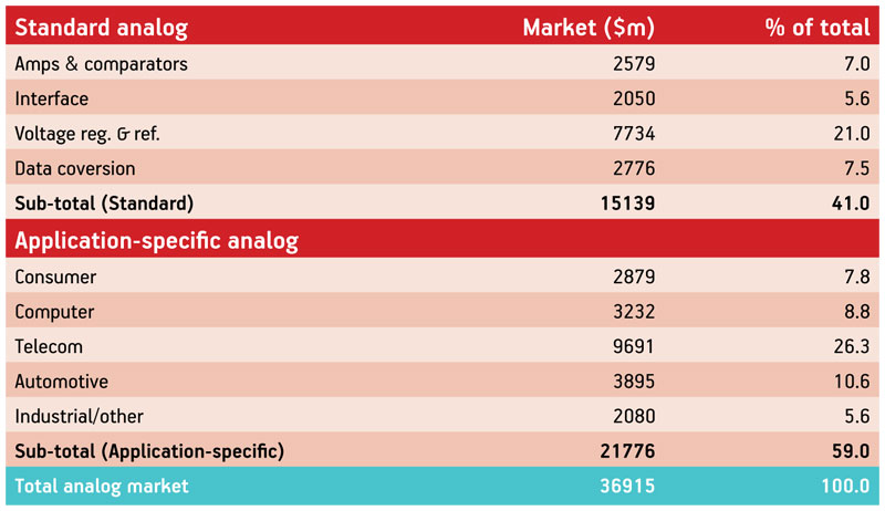
Figure 1
2010 analog IC sales forecast
Clearly, the larger players (e.g., Analog Devices, Linear Technology, Maxim, National Semiconductor, and Texas Instruments) have patent portfolios a mile deep. Those that engage in analog ASIC development also set the bar high as to whom they will work with. Typically, they have very large minimum-order requirements. For example, TI focuses its application-specific analog business on a small number of big customers like Seagate, Sony, Samsung, Hitachi, Toshiba and a few others. Their required annual unit and dollar volumes force the majority of the smaller customers to seek out independent analog or mixed-signal ASIC design providers.
As they embark on finding the right design provider, customers should take note of some of the following myths surrounding analog ASICs.
Myth 1.
“It is only economical to integrate analog functions into an ASIC if the analog content is minimal.”
The ASIC concept began as an integration strategy for lowering the costs of computationally heavy logic circuits. Today after more than three decades in use, ASICs remain heavily digitally oriented. When we hear the terms like system-on-chip (SoC) and intellectual property (IP) reuse associated with ASICs, we generally think of massively complicated, digital-centric devices that may also contain a few important analog functions. Historically, these products have established a mindset among the user community that a little analog can go a long ways. But what about applications that require analog-centric ASICs?
These are SoCs as well, even though they may not contain a processor core or even memory. Yet most ASIC companies are quite unprepared for the challenges of hand-crafting the unique analog circuitry required for important applications in such areas as healthcare.
The actual manufacturing cost of the ASIC chip may imply a huge savings when compared to the combined costs of the standard ICs it replaces (Figure 2, p. 46). However, there are other costs associated with the ASIC that must be considered and amortized over the life of the product. Non-recurring engineering (NRE), based on the complexity of the design as well as hard tooling costs such as masks and test hardware, can add a few pennies or even a few dollars to the final bill, depending on the complexity and lifetime volume of the device.
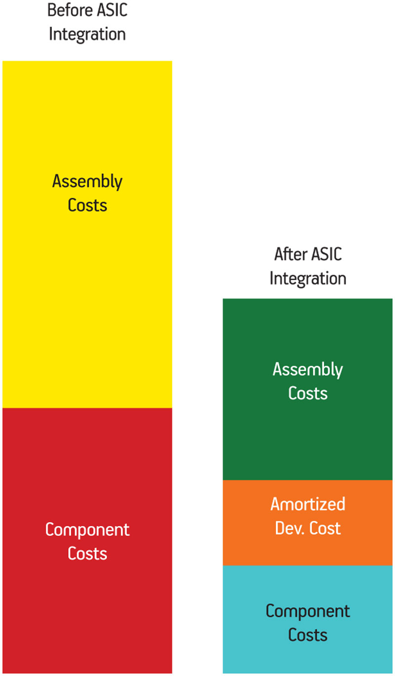
Figure 2
Total system cost
Incorporating elements that require more exotic processes for features like high current, low noise or high frequency will increase the cost of all the elements in the chip. Therefore, it is as important to know what to integrate into the ASIC as it is to know what functions should still be served by a discrete component. Interestingly, the use of multiple smaller, less complicated analog ASICs, differentiated by their manufacturing processes, can offer stunning cost reduction results.
Most analog applications use a collection of passive elements and discrete transistors in addition to the ICs involved. Integrating as many of these components as possible within the ASIC often comes for free and can have a dramatic effect on reducing the end product’s total assembly cost. It is often the potential total system cost savings that finally justifies development of an analog ASIC.
Myth 2.
“‘Mixed-signal ASIC’ means the same as ‘analog ASIC’.”
While the term ‘mixed-signal’ implies the integration of analog and digital circuitry on a single chip, there are distinct differences in the skills required to combine (analog and digital) library cells on a silicon chip and those needed to create an analog design that fully satisfies all the requirements of a specification.
For some applications, analog library cells offer sufficient performance. However, it is more and more frequently the case today that the inherent sophistication of the target analog application necessitates a design that is truly ‘application specific’ and not just a compilation of general-purpose blocks (Figure 3).
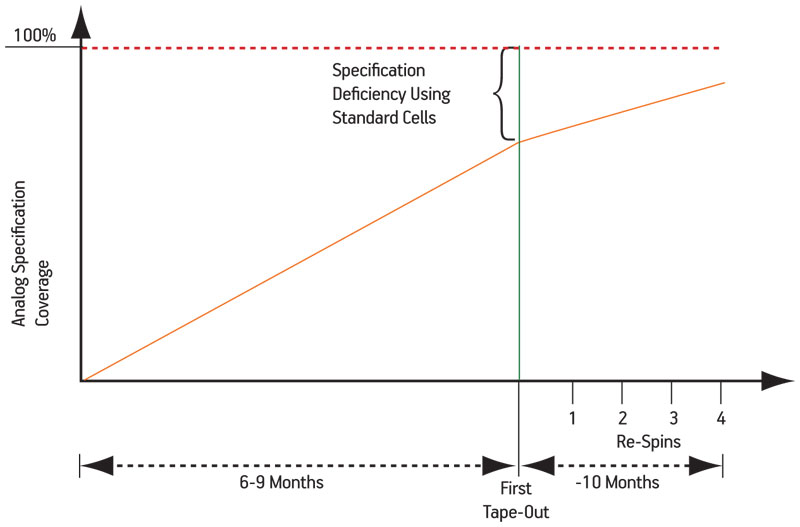
Figure 3
Typical inherent errors in achieving analog specifications when using standard mixed-signal cells
Like the big analog IC companies, true analog ASIC companies employ experienced designers, artisans. Many have spent years working at bigger analog players, learning from the industry gurus. So, do not let a mixed-signal design house negotiate you away from your ideal specification. Close isn’t good enough. Analog must be exact.
Myth 3.
“Only ultra-high-volume applications benefit from analog ASICs.”
As noted earlier, many large semiconductor companies focus their ASIC efforts on a handful of very large customers. These are the privileged few and everyone else must seek out development and manufacturing partners that match their needs. Almost all full service ASIC houses have their own business criteria regarding the minimum NRE, tooling and, most important, annual volume. Some do avoid the issue by just offering design services and leaving manufacturing to the customer. Either way, it is often the subcontract wafer fabs rather than the ASIC companies themselves that dictate annual volume entry levels.
The semiconductor industry operates in alternating cycles of boom and bust. A brief look back in time reveals that in boom times, capacity at the big Asian foundries fills quickly and all but the most promising, high volume customers are turned away. Aggregators have somewhat mitigated the problem by combining numerous smaller company requirements under the umbrella of their larger purchasing power. However, the large Asian fabs are built to benefit from economies of scale, offering processes tailored for the mass market: high density, lower power logic. For many, analog is problematic. Fortunately, there are bountiful alternatives.
Throughout the world and particularly in Silicon Valley, numerous boutique wafer fabs specialize in analog processes and are not loathe to accepting lower volume business. Considered a well-guarded secret, these fabs welcome low and moderate volume business while offering prices that are competitive with Asia’s multibillion dollar foundries. These smaller fabs have come to realize that while analog designs are often focused on lower annual volumes, they are generally less susceptible to the violent supply/demand curve swings inherent in the general semiconductor industry. Moreover, analog chips can sometimes remain in production for a decade or longer. For the fabs, accepting reduced annual volumes becomes an annuity that offers payback for years to come. Experienced analog ASIC design houses have spent decades nurturing these relationships for their customers.
Myth 4.
“Using existing IP from analog cell libraries lowers chip cost.”
Using predesigned, functional cells such as amplifiers, converters and transceivers can shorten development time and therefore have a ripple effect of lowering the chip’s total cost. However, even though design time is reduced, other tradeoffs must be considered. Standard analog library cells do not pack as neatly as digital ones. Using analog library cells can result in blocks of unused silicon on the die that needlessly lowers the number of potential die on a wafer (Figure 4).
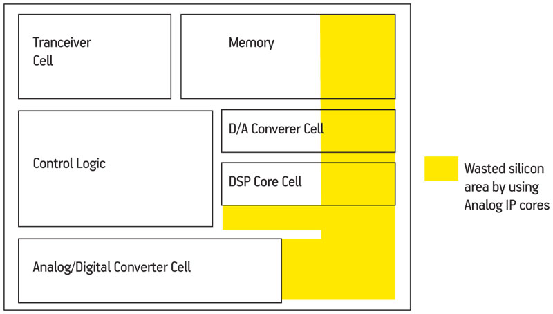
Figure 4
Layout using standard analog IP cells
Additionally, since the analog circuitry of a mixed-signal ASIC is likely to be the input and/or output of the circuit, these cells must be oriented closer to the periphery of the chip to facilitate easy access to bonding pads.
Handcrafting some or all analog functions allows the designer to accomplish several things. In a mixed-signal design, handcrafted analog circuits are laid out to fill voids created when using standard digital cells, better optimizing overall silicon area utilization (Figure 5).
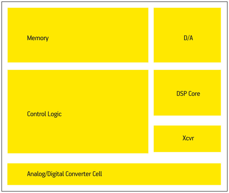
Figure 5
Layout using hand-crafted analog
Moreover, handcrafting the analog portion allows the designer to determine precisely the performance parameters of the circuit rather than restricting them to the fixed performances of a limited number of standard cells available in a library.
The conundrum of using overdesigned cells is another consideration worthy of the designer’s attention. For example, some analog parameters may be able to be relaxed for a given application, simplifying the handcrafted design compared to a standard cell. Alternatively, handcrafting the analog circuitry gives the designer the ability to improve other performance parameters that can have far reaching implications that make the ASIC less costly in terms of test yield and thus more competitive.
Myth 5.
“Cell-based ASIC designs ensure product differentiation.”
Designing the analog portion of a mixed-signal ASIC using a cell library is tantamount to designing a system using standard, off-the-shelf, analog IP with one key exception—selection. At the board level, there are tens of thousands of IC amplifiers, voltage references, converters and more from which to choose. In a cell library, the designer is limited to choosing from a few dozen. Performance compromises may be needed to accommodate these limited choices.
Analog-centric ASIC development affords a perfect opportunity to rise above the competition. As noted earlier in this paper, nearly 60% of the worldwide analog IC market is ASICs. If you and your competitors are basing your designs around the same mixed-signal cell libraries, both of you will have approximately the same performance specifications, dictated by the specifications of the library cells.
True product differentiation comes from invention. It is derived by bringing a uniqueness to a product that is not readily available to the competition. Cell libraries fail to deliver the necessary uniqueness often needed in critical analog applications.
Myth 6
“Handcrafted analog is too expensive.”
There are times and places where standard analog cells are more than adequate. Experienced design houses recognize this and only offer full custom analog when the specification merits it.
Handcrafted analog can create the differentiation required to break out of the pack with a superior performing chip and thus a superior end product for your customer. Additionally, stepping back from the cell library approach opens up options for manufacturing, since libraries are typically developed for one process at one fab. Broader-use libraries are available that specify a process (e.g., 0.35um CMOS) but have relaxed specifications such that they can be instantiated in multiple fabs.
Handcrafted analog gives you an unlimited set of manufacturing options, especially through the use of boutique foundries. Many of the boutique fabs differentiate themselves by the variety of services they offer and their willingness to make adjustments to their processes to accommodate optimizations to the chip’s performance. A recent example is a circuit JVD developed for a major automotive component supplier. The chip required a high voltage MOSFET that was not available in the boutique foundry’s standard process. Integration was critical to the success of the project, so the foundry and JVD worked together to create the needed device structure. The subsequent design provided the high voltage robustness needed for the application while minimizing parts count and the physical size of the end product.
NRE costs are a compilation of several variables. These costs must be amortized over the number of chips produced during the lifetime of the product to determine their effect on the unit cost of the ASIC. When executed properly, NRE costs associated with handcrafting the analog circuitry return a disproportionately lower unit cost of the final chip. The key to success is the analog experience resident at the ASIC house doing the integration.
Myth 7.
“The most cost-effective solution is to pack as much as possible into the mixed-signal ASIC.”
Insufficient analog expertise can get a mixed-signal ASIC house and their customers into a real bind. Missing a product launch window by a year or more is the kiss of death. When the analog component of the design is critical (i.e., more than a basic analog-to-digital or digital-to-analog converter), it is best to seek out analog ASIC experts to perform the integration.
Moreover, splitting the functions into multiple chips should be considered when both the analog and digital content is excessive. The fact remains, analog circuits perform better in non-digital fab processes. When the option is there and viable (from a cost/yield/board space perspective), the long-term cost benefits of a dedicated analog ASIC chip can be overwhelming.
Conclusions
The application will always determine the appropriate combinations of technologies that are best suited for the ASIC design. As we increase our dependence on cognitive prosthesis devices (e.g., smart phones, Wii controllers, tablet PCs, etc.), copper tethers disappear and analog increases its dominance in ASIC designs. MEMS advances have placed Star Trek-style sensors in our daily lives. Medical imaging, sensing and monitoring continues to improve healthcare provision. All of these and more increasingly rely upon better, faster, denser analog circuit content.
When considering a new ASIC design, carefully consider the role analog will play in its deployment. To minimize risk, choose your ASIC development partner carefully. Most of the time, mixed-signal ASIC design skills will be sufficient. But to minimize risk, seek out an analog ASIC partner with the right analog design skills and experience to match the application.
JVD
2266 Trade Zone. Blvd.
San Jose
CA 95131
T: +1 408 263 7704
W: www.jvdinc.com
