Cortex-A72: microarchitecture tweaks focus on efficiency
ARM has revealed a number of details of the microarchitecture that underpins its flagship Cortex-A72 as the processor moves towards its production release.
Back in the dim, distant past of the 1990s when monster superscalar processors first roamed the earth the emphasis was on the pipeline and how many execution units were being deployed, just as long as an out-of-order decoder and scheduler could keep them fed.
Fast forward to 2015 and the emphasis is very different. Energy controls the design. The emphasis in microarchitecture has shifted to often subtle tweaks that help the processor make best use of those parallel units but not if the decode and execution units needed to keep the beast fed start running hot enough to cook an egg.
ARM has revealed a number of the microarchitectural changes the company has made for the Cortex-A72 in an attempt to bring a major upgrade to the performance offered by the A15 commonly used today with greater power efficiency.
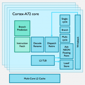
Image The main blocks used by the Cortex-A72
The aim of the Cortex-A72 is to provide the performance of a Cortex-A15 but at lower frequency, with that, lower voltage, as well as offering the possibility to push performance higher so that a 2.5GHz Cortex-A72 CPU consumes 30 to 35 per cent less power than the 28nm Cortex-A15 processor but delivering more than two times the A15’s peak performance.
There are a number of common elements in the tuning of the A72 microarchitecture that look to have homed in on the bigger energy consumers in processing, such as accesses to large memory blocks and internal bus transactions, and knocking out spurious operations that have a high probability of not resulting in any useful work being done. So, the stars of the A72 are not those doing the computation but the array of support logic that attempts to sift and stuff instructions into the pipeline as quickly as possible.
Branch-prediction changes
Branch prediction has been a key part of RISC processors for decades. Just about every processor with a decently long pipeline at least works on the assumption that a backwards-facing branch will be taken most of the time – and so will fetch instructions from that destination address as it nears the branch itself. Forward-looking branches tend to look more random so engineers have had to trade off large branch-history buffers, which consume a fair amount of energy on each access, against the performance and energy cost of having to dump the predicted instruction stream and grab the alternative.
As the A72 can dispatch up to five instructions per cycle into its eight-slot wide pipeline, unexpected branches have a major impact on throughput: it can take a number of cycles to kill off the predicted instructions and refill the pipeline even if the code is sitting in level-one cache. The company has fine-tuned the prediction algorithm using real-world workloads to better assess when a branch will be taken or not under various conditions.
The ARM engineers took the view that a more complex branch predictor than the one used on the A57 would offer a better trade-off between power consumed by the predictor itself and the energy wasted on mispredicted branches. ARM has increased the overall capacity of the history of taken branches, worked on algorithms to better predict outcomes, and reduced aliasing, a consequence of the limited number of address bits used to look up the history of a branch that can lead to the results of more than one recent branch being mapped to the same entry.
But, to reduce power consumption in situations where branch history has limited value and cannot effectively predict outcomes, the predictor does not get used at all. Heuristics determine whether the code falls into that category or whether it has the profile of a segment that would benefit from branch prediction.
The branch predictor also feeds into an optimization designed to reduce the power used by instruction-cache lookups. To help prevent data being unnecessarily flushed from the cache because it’s been overwritten by other entries that map to the same cache address, the Cortex-A72 has a three-way cache. Traditionally, any address lookup has to be done in parallel to all three sections, consuming three times the power compared to a simpler direct-mapped cache for that operation. The branch predictor directs the first attempt at a lookup to the way-section most likely to contain the data needed rather than firing off all three each time. Further help comes from an optimization that uses an early lookup and compare in the tag-RAM.
Memory splits for energy
Other areas of local memory have been split to reduce the power of accessing individual arrays. These include the translation lookaside buffers (TLBs) used to perform virtual to physical memory address translation and the branch-target buffers (BTBs) that hold instructions at the destination of previously taken branches. The regionalization of these buffers is done so that the upper bits can be disabled for the frequently encountered cases when page lookups and branch targets are to code and data that are relatively close to the areas used by currently running code.
Other areas where the A72 tries to avoid loading up highly capacitive arrays are in the often power-hungry register files used for speculative execution from instructions that lie beyond a predicted branch but which has not actually been taken. The team has significantly reduced the number of ports into these files as well as their overall area. Similarly, when instructions are finally dispatched and retired, additional logic is used to suppress accesses to the register file when operand data is known to be sitting in the forwarding network that funnels data from one instruction to another.
The focus on power has resulted in a shift towards greater complexity for individual operations. ARM, like many other processors, converts its core instructions into micro-ops that are generally simpler, but not always. The A72 works with more complex micro-ops and will even fuse the operations needed by two instructions together if they can be usefully combined into one micro-op. A number of buffer and flow-control optimizations have been made throughout the instruction decoder to cut the power needed for decode. The information provided by the decode unit also drives a number of power optimisations across the processor.
Load optimizations
To try to feed data more efficiently to the processor pipeline, ARM has redesigned the load/store unit and provided a more sophisticated prefetcher than previous microarchitectures, able to recognize more types of data stream which should result in more data sitting in either the L1 or L2 cache when it’s needed.
The load/store unit also allows power reductions by using a hit predictor for the L1 cache – avoiding accessing it if the predictor does not indicate that the data is in that cache. The processor also detects when the L2 cache is idle so that it can reduce power to the array until it is needed again. ARM claims the combination of the new pre-fetcher and other changes enable an increase of more than 50 per cent to the processor’s overall memory bandwidth.
For signal-processing and graphics work now typical of mobile-consumer designs, ARM has decided to reduce the latency of floating-point operations. The latencies have been cut by 25 to 50 per cent with the multiply-accumulate seeing a cut of 33 per cent to six cycles. The constituent multiply and add operations each take three cycles in the A72 from start to finish. Again, the emphasis is on keeping the pipeline fed: lower latencies mean integer instructions waiting on the results of those instructions are less likely to be stalled.
Benchmark workloads
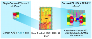
Image Area comparison of A72 and Broadwell core provided by ARM
ARM says the change contributes to a performance increase for the SpecFP and SpecFP2006 benchmarks of approximately 25 per cent. JavaScript should also show an improvement because the main datatype used by the weakly typed language is a double-precision float.
Although one of the prime targets is in high-end mobile, ARM has been telling analysts that the A72 will compete favourably with Intel’s Broadwell-based offerings for dense servers by fitting more cores into the same area as the x86 designs and with lower power consumption for multithreaded workloads. Using the die shot presented by Intel at last year’s IDF, using the TSMC 16FF+ process ARM reckons four A72s and 2Mbyte of L2 cache can fit into the area consumed by the Broadwell Xeon D and 256Kbyte of L2 cache.
Using comparisons with the existing Haswell-based E5 Xeons from Intel and assuming a 20-thread workload, ARM claims a 20-core A72 design can match the performance of a 10-core E5 2660 but at a third of the power consumption, although ARM’s calculations do not include the I/O power that was included in the tests on the Xeon. The ARM design assumes the use of the CCN-508 interconnect and a total of 28Mbyte of L2 and L3 cache. Overall, the A72 is likely to see more overlap with x86 than ever before.

