Analog verification IP and the next stage in the evolution of system-on-chip
Introduction
Considerable effort is being exerted to improve the quality and success of system-on-chip (SoC) designs. Given the demand for more and more features, lower power requirements, and need for blazing speeds to handle increasing data for video and other hungry applications, it is no surprise that complex SoCs are becoming harder to verify. A comprehensive test and verification strategy is vital; otherwise first silicon success is unlikely and precious financial resources are wasted.
Today’s large SoCs can contain tens of millions of gates and require the combination and reuse of intellectual property (IP) blocks for memory, processing and high-speed I/O. Using such blocks can dramatically accelerate development. This cuts the demands on internal resources required to develop an entire design. Engineering teams can focus on the unique value they add to a project while third parties (or other internal design groups) assist with more generic tasks.
Also, the growing use of high-speed serial I/O for computing, consumer and storage systems is bringing significant advantages of higher performance, reduced pin counts, and lower power consumption to entirely new markets, particularly compared with earlier generation parallel interfaces. However, these latest interfaces, which typically operate at 1.5-3.125 Gbps, must also meet gigahertz performance metrics signal integrity requirements and time-to-market schedules.
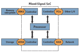
Figure 1. The use of several high-speed interfaces is now typical in SoC design.
Figure 1 helps illustrates the scale of the task involved. It shows a typical SoC which has several types of I/O: DDR and DDR2 for memory, XAUI for networking, Serial ATA for storage, and PCIe to connect various sub-systems to the main processor. A critical point here is that, to ensure SoC success, this third-party IP must be verified in the eco-system of the particular design within which it is deployed.
In the digital domain, this task is being addressed by the rise of testbench automation software that dovetails with the use of hardware description languages (HDLs).
HDLs provide more abstract design descriptions for entry, verification and synthesis but initial attempts to verify such designs involved writing testbenches in the HDL language of choice, exercising the design or device-under-test (DUT), and observing the results. This could be a cumbersome process.
Often designers and verification teams were writing 10 lines of verification code for every line of HDL. The step towards testbench automation software has reduced the size of verification decks to 10% of their original size, and provides data representations that elegantly describe the kinds of transactions digital and IP blocks were expected to perform. A typical example would be a testbench to verify correct processing of a SATA controller.
Thus, digital designers reaped such benefits as the reuse of testbenches for later generations of a design, easy testbench modification in the case of feature and specification creep, and access to a systematic methodology that could take advantage of new verification technologies. In particular, the dynamic checkers in testbenches could be mapped to formal assertions for proving the correctness of digital designs. However, this model does not extend greatly into the world of mixed-signal SoC verification where high-speed I/Os or other blocks of analog IP feature. Indeed, the industry simply has not had an equivalent form of testbench automation for analog and mixed/signal designs.
The analog challenge
In the world of high-speed SoC design, digital signals exhibit analog behavior. Designers must concern themselves with the electrical performance of circuits running at gigahertz frequencies and implemented in nanometer IC geometries. Moreover, the requirements for verification are even higher than for digital blocks, since many more environmental and physical effects and parameters must be taken into account.
The list of such concerns is long. It includes signal integrity, powersupply noise, and reaching robust performance targets within process, voltage and temperature variations. Interconnect and device parasitics from a routed design can have a tremendous impact on circuit timing and lead to a failure to meet performance goals. When generating these gigahertz interfaces in-house, design teams have brought on board high-speed analog ‘gurus’ to ensure the success of their designs. These experts typically boast years of experience that enable them to eventually create successful designs using their own tests and methods, but they have not really introduced (or laid the ground for) any automation of their methods. Their tests and testbenches tend to be one-off scripts, suitable only for a specific design and development environment, and understood only by their creators. They are not transportable to other designers or other design teams that may use this interface IP. In addition, it is worth noting that analog engineers are hard to come by and their time is much better used designing rather than writing verification scripts.
Meanwhile, those design teams with no in-house analog expertise to assist in creating these high-speed interfaces, have, quite naturally, looked to IP suppliers who can provide the physical layer (PHY) interfaces. However, this can raise many similar issues. Whether using third party or in-house interface IP, verification must be done to ensure the success of the design. Designs do have bugs (features you didn’t expect). Anyone using an IP module must have some understanding of what was tested in the IP and how it was done.
Even more importantly, one should know what was not tested. This is because compliance to a standard only covers those situations that are covered by the standard. Often design teams will need to handle or verify operations outside the standard to improve the robustness of the design across all operating conditions.
The level of complexity of these high-speed interfaces means verification can be done in-house using SPICE or Fast-SPICE simulators. However, the time and expertise to setup the tests and run them is often not available. The availability of verification IP for these interfaces would add much needed rigor to the process, fully document what was tested and create confidence that the design will be right first time.
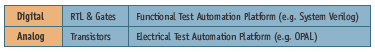
Figure 2. Analog verification IP requires a platform similar to digital verification IP.
Verification IP for AMS
Verification IP for digital modules has been available for some time. It consists of testbenches, checkers, and assertion-based verification that can be passed on to customers to verify performance inside a particular SoC design using Verilog/VHDL simulation. There is a corresponding need for the equivalent verification IP for analog and mixed-signal blocks, as shown in Figure 2.
High-speed interfaces are a combination of analog and mixed-signal digital blocks. Design teams are organized by expertise with digital designers using digital design tools and analog designers using their brains in combination with SPICE circuit simulation. This partition of the design effort can lead to problems about who owns the analog/ digital design interface and, then, in verifying the assumptions the two sides are using. Nevertheless, rigorous verification of this interface will catch imprecise specifications of timing margins, or functional changes in the behavior of logic control signals.
The operating environment for these interfaces – from their on-chip power supplies to transmitter/receiver, through the link across the package and traces of a printed circuit board – presents a number of challenges. Examples include tackling line losses; avoiding impedance discontinuities that cause signal reflections, simultaneously switching outputs (SSO), and crosstalk from line-to-line; ensuring robustness with regard to electro-static discharge (ESD); achieving acceptable yield across IC manufacturing variations; and staying within jitter, bit-error-rate and power budget specifications.
A comprehensive verification methodology must therefore address both the AMS and digital domains. For pure digital verification of the PHY within the SoC, digital behavioral models of the AMS sections are used to assure overall system functionality, or, as an alternative, one can apply AMS or co-simulation environments that combine digital blocks and analog components in a single simulation.
To verify the timing and signal integrity of the PHY for setup/hold and jitter margins through the entire data stream requires considerable analysis across variations in process voltage and temperature.
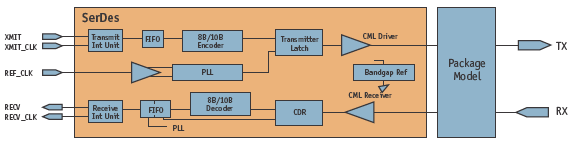
Figure 3. A typical PHY architecture using a serializer/deserializer for high-speed I/O.
A typical PHY architecture is shown in Figure 3. Here, the transmit and receive channels are connected to form a single line. Detailed circuit simulations using SPICE or Fast-SPICE engines are performed to get the analog electrical performance of this signal chain.
The newest generations of PHY IP now include built-in hardware tests for evaluating link performance and signal margin post-silicon. However they still do not remove the need for testing the design’s analog performance before manufacture, taking into account package model, trace length and noise injection. Nobody wants to wait until the chip comes back from manufacture and is placed in the hardware tester to discover that the interface performance is inadequate or that the eye is closed.
A platform for electrical verification is the best way to achieve robust, rigorous, economical and automated verification of these complex analog and mixed/signal blocks. One example of such a tool is Knowlent’s OPAL electrical verification platform (EVP).
OPAL EVP
OPAL EVP provides several distinct features to automate the verification task.
- The platform encapsulates and performs all analog tests listed in the IP specification. Some of these can get very complicated (e.g., recovering an embedded clock or measuring jitter and breaking it down into deterministic, random and periodic jitter components).
- The platform helps run these tests across multiple corners to cover the solution space and effectively manages the data for what can easily be 1000 simulations. Porting the testbench across to a different process, foundry or simulator can be done in minutes instead of weeks or months.
- The automation of the specification verification eliminates guesswork through a standards-based methodology. And the investigation of parameter changes is easily achieved for any test, allowing drill-down for design issues.
- A complete compliance check against specifications prior to fabrication prevents silicon, package and board re-spins.
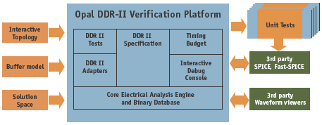
Figure 4. OPAL verification IP platform for DDR-II memory interface.
The OPAL EVP for DDR-II, the de facto memory interface standard, is shown in Figure 4.
For the IP developer, all testbenches are complete and specific for the required PHY interface. Test vectors and passive load models for the specific IP and the data collection of simulation results are already included in the platform and cover all DC, AC and transient mode tests. Binary database processing of simulation data provides the fastest throughput possible, and avoids slow, ad hoc data collection using specific simulator directives such as measure statements in the SPICE deck. Debug analysis is easy and efficient, and takes advantage of existing SPICE and Fast-SPICE simulators in the design flow. The designer now has tremendous leverage over the tests and net lists used to verify the design.
Integrators of the PHY layer IP are not usually interested in the specifics of the implementation of the protocol. Their primary concern is that the IP is compliant and will work in their specific design. OPAL EVP provides the means to perform compliance testing of the IC package, channel and PCB interconnect. The platform is designed for the most efficient investigation of crosstalk and signal integrity effects, package choices such as wirebond versus flip-chip, and eye-quality versus trace length. Power management schemes can also be investigated to determine if low-power or standby modes of operation are working correctly.
Automation of analog/mixed-signal IP verification is the next stage in the evolution of successful SoC creation. Instead of designers enduring partially verified high speed I/O’s and multiple re-spins because of unacceptable electrical performance, the automation of IP verification removes the tedious, manual and error-prone process of test development and enables better, robust and more intelligent design.