The advantages of MIPI specifications in mobile, automotive and multimedia applications
A look at the ways in which the evolving MIPI standard is being used to provide connectivity in automotive, mobile, multimedia, virtual reality, augmented reality and related applications.
The pace of the mobile market has accelerated the development of standards that enable SoC designers to focus on what differentiates their work, rather than infrastructural issues that don’t set their designs apart. One of the most important of these is MIPI, a set of standards that make it easier to implement common features of smartphones such as displays and imaging devices.
The ubiquity and power of MIPI has not gone unnoticed in adjacent markets, especially those that are adding features such as image sensors and displays. These include the automotive market, which is using a lot more image sensors as advanced driver assistance systems, such as lane-keeping warnings, are implemented as cars evolve toward full autonomy.
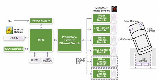
In a typical mobile application, an application processor uses a MIPI Display Serial Interface (DSI) and Camera Serial Interface (CSI-2) to provide well-tested, low-power, low cost interfaces to displays and cameras. The same architecture carries over into the automotive world, in features such as intelligent rear-view mirrors, wing mirrors and even surround-view systems. For these, a car with a camera on each corner, with a MIPI CSI-2 interface connecting the image sensor to the module. An Ethernet link would then make the longer-distance connections from the modules to a central processor, which would provide the ADAS functionality and drive a display over the DSI interface.
Figure 1 Example of an ADAS application using the MIPI DSI and CSI-2 specifications (Source: Synopsys)
A similar architecture can also be adapted for use in virtual-reality (VR), augmented-reality (AR) and mixed-reality (MR) displays, for use by the medical, industrial, maintenance, and home maintenance professions, and in consumer applications. VR, AR and MR applications are also using MIPI in various ways, such as in bridge ICs that connect to an arbitrary (DSI or other) display, do some image processing and then drive other displays through DSI links.
Basic multimedia processors are also being developed that use the MIPI CSI-2 interface to connect multiple cameras, and I3C, an upgrade to the I2C and serial peripheral interface (SPI) standards, to connect multiple sensors. More powerful versions of these processors would also receive inputs from, and drive, displays over DSI links.
Advantages of MIPI CSI-2, DSI and I3C
MIPI CSI-2 is a high-bandwidth interface between cameras and host processors. Data is transmitted using differential signals, with a dedicated clock, and the physical layer of the interface is a D-PHY, also defined in the MIPI specs. MIPI also specifies a Camera Control Interface (CCI), which allows read and write access to the camera control registers.
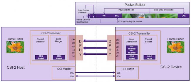
Let’s go through a simple illustration to see how data gets from the sensor to its host system using CSI-2. Given that the image is held in a frame buffer (see Figure 2), a packet builder will take one of the lines from that buffer and start building a packet. in doing so it will also index the packet header, the first field of which holds the virtual channel information, so each packet can be tagged as belonging to a particular data stream. This enables multiple streams of data to flow over the same link, using the virtual channel identification to distinguish which stream each packet belongs to.
Figure 2 How MIPI moves sensor data using CSI-2 (Source: Synopsys)
The second field defines the data format (RGB, YUV or RAW), the word count, and an error correction code (ECC) code to protect the header information. After the payload of image data, there is a CRC field.
The finished packet is passed to the lane distribution system, which works with MIPI D-PHY and converts the CSI-2 packet into multiple D-PHY high-speed bursts which are sent across the physical link. At the receiving end, the packet is received and sent to the packet decoder where it is checked, errors are recovered and the resultant image data sent to the receiving frame buffer. The process continues until all the data lines have been transferred. MIPI CSI-2 uses short packets for frame events, and long packets for the image data. Between each packet, the link goes into a low-power state in which it remains until more data needs to be sent.
MIPI DSI – the display serial interface
DSI is a high-speed serial interface between a peripheral and a host processor, receiving parallel data from the host and serializing it. On the receiving end, the reverse process happens to recover the parallel data. The DSI host will encapsulate the pixel data and control information into a packet format and send it to a display.
There are two main operating modes in DSI – command mode and video mode. In command mode, it is assumed that the display has a local frame buffer to which the host can write. The host uses command mode to write to or read from the register and frame buffer memory by using DCS commands or other vendor-defined commands. In video mode, the host transfers a real-time pixel stream to the peripheral, which expects a constant flow of video data and synchronization information. MIPI DSI defines packets not only to transport pixel data, but also to transport the event information (vertical sync, horizontal sync).
Display Pixel Interface (DPI) specification defines video formats and signaling for displays. It’s similar to a simple RGB interface where timing signals like vertical and horizontal signals are transmitted together with the video lines pixel information to define the format resolution and refreshment parameters. When the host side is driven with a DPI interface, the packet builder will detect the rising edge of a vertical sync signal and create a packet that includes detailed information indicating that it is a protocol sync event. As in CSI-2, the packet will be sent to a lane distribution controller, where it will be converted into D-PHY packets and sent across the link. At the other end it will be recovered, and the event will be sent to the logic that is driving the display. A similar thing happens with the horizontal sync signal.
This creates a data structure that represents an image frame with the associated horizontal and vertical sync signals, image data and blanking periods. These blanking periods can then be used in a number of ways, for example to send the link into a low-power state, to carry non-video packets, such as display configuration data or video packets for a different virtual channel.
MIPI I3C – a faster, scalable sensor connectivity
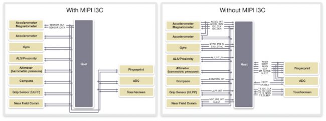
Today’s smartphones typically have 10 to 15 sensors, which together require up to 18 pins to connect. They are usually connected with a mix of I2C and SPI, using I2C for the lower data-rate sensors and SPI for the higher data-rate ones.
This approach requires multiple sideband signals, for example for interrupts, chip selects and enables. There’s no standard driver for all these fragmented interfaces, increasing the package size and adding complexity which translates into additional costs.
MIPI I3C solves these issues. It builds on the two-wire simplicity of I2C and the high-speed, low-power nature of SPI and adds features such as in-band interrupt, built-in command support, dynamic addressing, advanced power management, and high data rates, while maintaining backwards compatibility with I2C sensors.
Figure 3 How I3C can simplify a sensor subsystem (Source: Synopsys courtesy MIPI)
An I3C system can include a main master (of which there can only be one) and secondary master(s), which can ask to take over the bus ownership from the main master. There are also I3C slave(s) and I2C slave(s).
The two-wire interface can run at up to 12.5MHz, with an SDA signal, which is a bi-directional data port, and SCL, which can be used either as a clock port or as a bi-directional data port in high data-rate (HDR) modes. Only the current master can drive the SCL signal, which is always driven in a push-pull fashion.
Additionally, there are three versions of I3C’s HDR mode. HDR-DDR, for dual data rate, uses the same signaling strategy as SDR but runs at about twice the speed. HDR ternary symbol legacy (HDR-TSL) mode uses ternary coding to achieve higher data rates on buses that carry a mix of I2C and I3C devices. A further variant of this is ternary symbol plus (HDR-TSP), which uses ternary coding at higher data rates on buses connected to I3C devices.
Devices need several features to exist on an I3C bus. The first is either a provisional 48-bit ID, or a static address. The second is a device characteristics register. To initialize an I3C bus, its main master has to know the number of devices connected to the bus that will need a dynamic address, the information about I3C devices that already have static addresses, and the information about legacy I2C devices on the bus.
The master provides a dynamic address to a device when an I3C bus is initialized, or when the device is connected to an I3C bus that is already initialized. The main master sends a broadcast command code ‘enter dynamic device assignment (ENTDAA)’, and assigns dynamic addresses to all the I3C devices on the bus including those that already have a static address.
During the ENTDAA procedure, the master assigns dynamic addresses using provisional ID and device characteristics data.
I3C transfers
There are a number of forms of I3C data transfer, all of which happen within a frame with a Start/Repeated Start and Stop. Legacy I2C transfers remain unchanged. SDR messages can either be broadcast, or go to a particular slave’s dynamic address. HDR messages are preceded by a broadcast message (enterHDR CCC) that tells all the devices on the bus that it is moving from SDR to HDR mode, so I3C devices that support HDR can be ready.
I3C slaves can request the master’s attention through an interrupt, initiated by the slave when it detects an idle bus, which sends a message to the master with its dynamic address. Slaves can also join the bus after it has been initialized (hot-join), by sending a command to the master that will trigger a new dynamic address assignment procedure (ENTDAA) that resets all the dynamic addresses that have already been assigned and restarts the assignment process.
MIPI D-PHY
MIPI D-PHY is used with MIPI display and camera interfaces in thousands of implementations, and is low cost, and low power. It is optimized for unidirectional high-speed transmission, although there is also a low-speed, lower power mode as well.
The D-PHY uses a forwarded DDR clock link architecture, with one clock line and multiple data lanes. Static or dynamic de-skew is supported through calibration, and spread-spectrum clocking is also supported to address electromagnetic interface (EMI)/electromagnetic compatibility (EMC) issues.
The D-PHY has steadily evolved to higher data rates, while maintaining backwards compatibility.
SoC design considerations
In designing an SoC with camera and/or display interfaces, designers have to consider the total resolution requirements, number of ports, and the application targeted, so they can make informed decisions about the number of ports to implement, the number of lanes per port and the rates at which each should run.
On the protocol side, designers have to decide on issues that affect the area, power and memory storage needs of the implemented interface. Decisions such as a shift from using version 1.1 of the D-PHY to version 1.2 could cut the number of pins used, the power and area consumed, and also whether the interface can compensate for signal skew. Architectural decisions can also be made that give the end SoC greater flexibility. For example, designs often use two CSI-2 host controllers to control a pair of two-lane D-PHYs to support two low-resolution image sensors. With the right architectural decisions, however, a single host controller can be put in charge of two D-PHYs as a start-up option, so it can then control the four lanes necessary to support a single, high resolution image sensor.
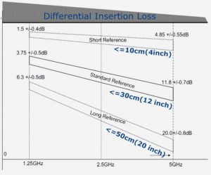
MIPI D-PHYs are built to support very short distances, as you might find in a mobile phone; challenging channels such as flex cables or chip-on-glass interfaces; and the longer distances that you would find in a laptop. The spec also supports static and dynamic de-skew, to manage signals over these more challenging channels.
Figure 4 Three reference channel models targeting different channel lengths (Source: Synopsys)
Automotive requirements
Although much of the MIPI spec is already suitable for use in automotive applications, in terms of its functionality, the way it is implemented represents another challenge for SoC designers.
Synopsys is already working on automotive-grade MIPI IP, which has been designed to meet the ISO 26262 functional safety requirements and to ensure designers reach their target automotive safety integrity levels. The IP is designed to have the reliability necessary to help cut the time it takes an SoC to reach AEC-Q100 qualification, and also meets the quality levels required by automotive manufacturers.
Further information
Web page: DesignWare MIPI IP Solutions
White paper: I3C white paper
Webinar: New Use Cases and Advantages of MIPI Specifications in Mobile, Automotive and IoT SoCs
Author
Licinio Sousa, technical marketing manager, Synopsys


