Advanced post-silicon verification and debug
More than 50% of highly complex systems-on-chip (SoCs) have functional issues at first silicon, issues that emerge after engineers have spent much time and money on verification and emulation. These issues delay time-to-ramp and cause significant losses of direct and indirect product revenue. All this demonstrates the need for efficient post-silicon debug methodologies and tools.
Post-silicon debug is a serious challenge. Only a few of the thousands of important internal signals are directly accessible and observable during normal chip operations. An important factor here is the limited number of pins of the SoC. A key objective of post-silicon verification and debug methodologies is to provide observability and control of as many internal signals as required, while keeping the area overhead and timing impact as low as possible.
Accelerated chip verification and debug, shorter product and system qualification, and earlier ramp-up capability are vital success factors provided by advanced post-silicon verification and debug methodologies and tools. The main component such tools require is a reconfigurable on-chip debug infrastructure for use at several stages of the development and during the lifetime of the chip. This article discusses the benefits of post-silicon verification and debug for products with short lifetimes.
DAFCA’s ClearBlue product suite contains software modules and debug infrastructure silicon intellectual property (IP) specifically developed to address the post-silicon validation challenges of nano-era semiconductor design. SoC design teams can incorporate the patented, reconfigurable fabrics during RTL development, enabling powerful at-speed debug, diagnosis and validation to accelerate validation and system bring-up with early silicon engineering samples.
Pre-silicon, the ClearBlue Instrumentation Studio software delivers a user-directed environment for insertion of the reconfigurable debug instruments (ReDI) into the SoC RTL. In the post-silicon stage, ClearBlue offers a wide spectrum of configurable, at-speed analysis capabilities, including trace buffers, logic analyzers, event- and assertion-based debug, and performance monitoring.
Observation, discovery and diagnosis
The observation, discovery, and diagnosis of functional issues at-speed, performed without adding extra pins or degrading nominal performance, is critical to post-silicon verification and debug. This is achieved by inserting a reconfigurable debug infrastructure at the RTL level and by dynamic reconfiguration during post-silicon validation and debug.
The debug intellectual property (IP) is comprised of a library of instruments, a generated signal probing network and a central debug module (Figure 1). An important differentiating feature of the technology is that it can configure the debug infrastructure post-silicon, allowing the flexible use of various debug applications as required by the actual debug situation.
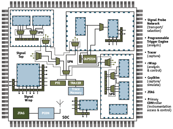
Figure 1. SoC block diagram with debug instrumentation
The debug infrastructure can be implemented in an ‘observe only’ mode with very low overhead – a lightweight fabric and simple multiplexer network that brings time-stamped bit-wise data to a central trace buffer. Alternatively, internal signals can be wrapped with a new form of reconfigurable logic that enables more sophisticated event-based debug, assertion-based debug, performance monitoring and even soft fixes of functional and timing issues that are discovered. This enables continued debug in the presence of ‘blocking’ errors.
The three main applications of this on-chip, at-speed debug methodology are:
- IP hardening. New IP blocks that have not previously been verified in silicon introduce functional risks. To mitigate these risks, users utilize the debug instrumentation to observe and analyze the functional behavior of IP blocks on-chip and at-speed.
- Platform chips. These are highly complex SoCs with multiple programmable cores and tens of millions of gates. The interaction of multiple bus hierarchies, clock and power domains make validation and qualification difficult and application-dependent. To mitigate this challenge, users apply on-chip debug instrumentation to observe and analyze functional issues including deep-state and intermittent issues. They then attempt to fix these though patches to the embedded software.
- Short-lifetime products. SoCs for consumer, PC and computer peripherals typically have lifetimes of a year or less. Smooth validation, qualification and ramp-up are essential to economic success. Users in this category deploy on-chip debug instrumentation to observe and diagnose functional issues and then either patch embedded software to mitigate the issue or apply quick partial mask-set re-spins.
The on-chip debug infrastructure can be applied at several stages of the development and life cycle of the chip:
Stage 1: Develop an instrumentation strategy
During this initial phase, the project team must identify those IP blocks or sub-blocks, busses and finite-state-machines that pose a high functional risk and/or should be the focus of diagnosis and debug. High risk is typically indicated by the implementation of new, not-validated silicon; hardened IP; IP that has been transferred from a previous technology node; IP with an unknown verification history; new interface and bus standards; finite-state machines in IP-blocks; and areas with low assertion coverage.
For each identified block, the signals that should be observed or controlled are identified. Signals marked for observation only will be tapped (no change to the signal path), whereas signals marked for observability and control are wrapped (insertion of a bypass multiplexer in the signal path). The result of this phase is a list of signals marked to be tapped and/or wrapped.
An important byproduct here is the analysis of the design/architecture for a functional risk assessment. This can be used to improve the flexibility and robustness of the system architecture and, thereby, the ease with which late changes can be made. It also guides the pre-silicon verification effort to improve coverage of the risk areas.
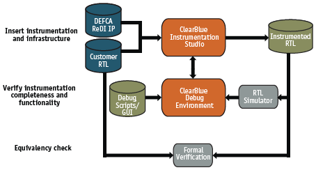
Figure 2. Pre-silicon instrumentation with ClearBlue
Stage 2: Instrumentation of the RTL
The debug and validation instruments are automatically inserted, followed by formal verification of the instrumented RTL to verify functional integrity of the original customer RTL (Figure 2). In addition, timing closure constraints and a testbench for the inserted instruments are generated that will support verification, physical design and timing closure. The result of this phase is verified, instrumented RTL.
Stage 3: Synthesis and timing closure
The instrumented RTL is synthesized using the customer’s target standard cell library, followed by timing closure and functional verification/simulation. The physical design is now ready for tape-out.
Stage 4: Tape-out and manufacturing of initial silicon
At this point the design is passed on for the manufacture of first silicon either internally or by the foundry.
Stage 5: First silicon, initial post-silicon verification and debug
In this first post-silicon phase, the on-chip debug infrastructure is used to analyze, diagnose and debug functional issues in the instrumented regions. The debug tool communicates via the JTAG port with the debug infrastructure. Tapped signals can be dynamically selected and observed. Wrapped signals can be controlled by configuring the inserted wrapper cells for functional and timing manipulation. Both signal groups can be linked to debug applications like event-based debug, assertion-based debug, performance monitoring, stimuli generation and response capture. In addition, the debug infrastructure enables soft-fixes of wrapped signals, temporarily correcting functional or timing issues, and allowing for continued validation and debug after initial functional issues have been identified. The result is a list of identified functional issues and corrective actions.
Corrective actions can be changes in the embedded software, functional changes of the design that require a metal re-spin, or in the worst case, a full mask re-spin. Ideally, the objective for short lifetime products is to implement as many fixes as possible through changes in the embedded software.
The key benefits of this phase are much faster post-silicon validation and debug time. The improved signal observability and configuration capabilities of the debug infrastructure benefit the development and validation of the embedded software by monitoring the actual performance of busses, memories and complex transactions. The debug infrastructure also allows effective verification and validation of embedded software patches.
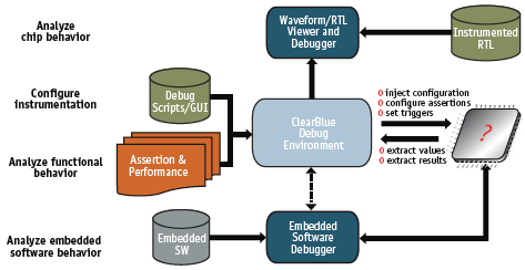
Figure 3. Post-silicon validation and debug
Another key benefit of the debug infrastructure is the ability to discover and correct deep-state functional issues or intermittent functional problems. These types of functional problems are the hardest to deal with. Pre-silicon verification cannot typically detect issues that arise only after millions of clock cycles have passed because of limited simulation time. Intermittent functional failures that may lead to system crashes after hours or days of operation are not addressed by traditional test and debug methodologies.
This debug infrastructure also provides assertion-based debug that enables the product engineers to monitor chip and system behavior over longer times and multiple operating conditions. The signal history stored in the embedded trace buffer then allows reconstruction of the events and operating conditions that lead to a problem, aiding the implementation of an efficient fix.
The result of this phase is validated silicon and embedded software.
Stage 6: Qualification of the validated silicon
The debug instrumentation is utilized for improved and accelerated qualification testing of the chip. This includes performance monitoring over voltage and temperature changes, assertion monitoring, stimuli generation and signal capture at-speed of high-speed IP blocks that cannot be directly observed (either because of access limitations or because high internal speeds preclude external observation).
Stage 7: Integration of the chip into a system (board)
The chip is tested in its final system environment and the system is qualified. The on-chip debug infrastructure can be utilized to diagnose functional issues in the system environment, allowing final adjustments in the system board or embedded software. This delivers better visibility and shaves weeks and months off test and qualification time. The result is a system validated and qualified earlier and with much better coverage and understanding of functional limitations.
Stage 8: Deployment of the system
The system with the debug-instrumented chip is deployed in the field/market, and ramp-up to production volume begins. Yield learning is critical at this stage for cost reduction and volume delivery capability. The debug infrastructure can be utilized to analyze functional yield limiters and to develop fixes or work-arounds.
Depending on the product, the debug instrumentation can also be used for in-field diagnosis and test. In addition, the debug infrastructure can be used for the diagnosis of functional issues of field returns.
The debug infrastructure has benefits over the complete lifetime of the chip and can help to significantly reduce post-silicon validation, debug and qualification times. These benefits far outweigh the cost of implementation.
Typically, the additional gate count for the debug infrastructure is in the range of 4-6% of the total gate count of the device, The additional delay incurred by wrapped signals is only one multiplexer-delay and in most cases is not critical: tapped signals have no additional delay beyond the one introduced by one additional gate load. The tool suite provides constraint files for timing closure and the capability to pipeline the signal probe network to ease routing congestions and timing constraints on the user-defined logic.
Summary
The described methodology is based on the insertion of a debug infrastructure at the RTL level, which then can be dynamically reconfigured post-silicon to adapt to actual validation and debug situations. It provides a set of effective debug applications that help to reduce post-silicon validation, debug and qualification times by several months.
DAFCA Inc.
10 Speen Street
Framingham
MA 01701-4661
USA
T: +1 (508) 663-3300
www.dafca.com
