Achieving better DFM: EDA tools pave the way to improved yield
Major yield-Inhibiting Issues At each successive process node, additional defect mechanisms appear and hinder the ability to achieve desired yield (Figure 1). The trend toward declining yields has led to a resurgence in the application of design for manufacturing (DFM) methodologies.Much of this reinvigorated effort relies heavily on a new breed of tools and technologies. But before designers adopt a comprehensive DFM methodology, it is important that those making the choice understand the primary causes of yield loss. The three more common ones are described as:
- Random
These are typically associated with particle defects. - Systematic
These are induced by the process or lithography applications. - Parametric
Here timing or other failures are a result of device physics and interconnect effects.
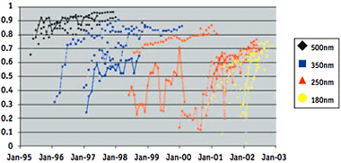
Figure 1. Initial production yeilds have not improved, and mature yields have declined
Random defects
Random defects are the dominant yield loss mechanism at larger technologies. Despite constant clean room improvements, particles still land on chips or masks. These particles cause catastrophic failures – shorts (extra metal between two metal lines) or opens (missing metal) – or result in parametric issues – resistive pinching, added coupling, etc.
Random defects are being driven down in conjunction with feature scaling in advanced processes, enabling a chip to maintain a similar yield as it undergoes a simple process shrink. At the same time, the increase in functional integration enabled by smaller features makes these designs even more susceptible to particle defectlimited yield.
Systematic defects
Systematic yield issues are not random in nature, but the result of interaction between the layout and process variations. These include chemical variations in materials; mechanical variations in CMP, optical variations in lithography; and plasma variations in etch. Some examples of systematic defects are: planarity (the difference in metal heights for a given area on a design), antenna effects (charge accumulation of interconnect components), via opens and electromigration.
A significant systematic effect occurs within the copper manufacturing process. Via opens, due to the copper cladding process, result from voids traveling down into the via. The results can vary from resistive via connections to completely opened lines. Some improvement to yield is gained by using redundant vias. If one via fails, the redundant via compensates for the failing one.
As features sizes have decreased, manufacturers have turned to resolution enhancement techniques (RET) to help compensate for the physical limitations of stepper wavelengths. But the ability to apply RET appropriately can be limited by the design layout itself.
Certain types of RET have requirements on pitches (a pitch is essentially half the width plus half the spacing of the polygon in question). Today, this is most problematic for poly gate transistors, but is quickly becoming important for metal lines as well.
Parametric defects
The biggest issue for nanometer-scale designs is considred to be parametric yield loss. This is when all elements of a chip are functioning, but timing or other electrical requirements, such as power, are not to specification.
Parametric defects became an issue at 180nm, grew dramatically in number at 130nm, and are of significant concern in 90nm designs. They are the result of interconnect parasitics and device physics, and can cause a circuit to behave in non-ideal ways, leading to effects such as power bus voltage drop, increased noise, and timing skew in clock and signal lines.
Designers need device parameter and parasitic extraction tools that capture complex silicon effects and account for them in the design. If not accurately simulated, modeled and handled, the impact of these defects can have dire consequences on the success of a chip.
Practical approaches to DFM in the nanometer era
While the sources of yield loss appear ominous and difficult to overcome, significant work is being done to help produce designs that are much more resistant to yield issues. Current EDA tool development is concentrating on several areas:
- Analysis of DFM rules.
- Yield enhancement.
- Physical test.
- Litho-friendly design.
- Nanometer silicon modeling.
Statistics come to signoff
Traditionally, design rule checking (DRC) has been one of the key communication vehicles between manufacturing and design. The DRC rules tell the designer the limits imposed on them by the manufacturing process. Most of these constraints represent true process limitations, which, if not followed, produce nonfunctioning silicon or lower yields considerably.
However, while traditional manufacturing constraints are easily quantified in DRC rules, yield issues are more difficult to pin down because they depend on a number of variables and are largely statistically driven (i.e. the greater the occurrence of a certain configuration, the greater the likelihood of chip failure).
Recently, foundries have started delivering ‘DFM recommended’ manufacturing rules as well as those for DRC. These new rules are given to designers to indicate where a design becomes easier to manufacture by adhering to the DFM rule, rather than the minimum spacing DRC rule. This all sounds useful in theory, but to a designer, the whole point of moving to the next process node is to take advantage of more aggressive minimum spacing.
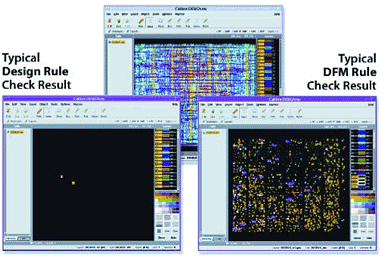
Figure 2. A simple DFM rule check may produce millions of errors. Designers need statistical methods for evaluating their impact.
The quest to comply with DFM recommended rules opens the door to many questions (Figure 2).What tools help the designer determine, for an area of the design, if DRC rules or DFM rules have a more positive impact on yield? One way is to gather layout statistics on the feature in question. For instance, statistical modeling and critical area analysis highlight show not only how often an issue occurs, such as antennas and vias, but also in which combination and level of severity.
Statistical models reveal what accumulative effect a yield issue has on an area as well as on the design as a whole. Armed with comprehensive statistics, a design manager can determine which issues have the most impact and which are cost effective to fix. In the future, tools must address this ‘DFM recommended rule’ data in terms of statistics, and not only provide information about the feature-based improvement in yield, but also a means to determine how these modifications impact the ‘litho-friendly’ and ‘timing-aware’ aspects of the design. New tools must also give designers a way to make yield predictions, allowing the designer to prove if modifications to the design ultimately resulted in better yields.
Automatic yield enhancement emerges
Clearly, the physical layout of a design has a primary impact on yield. The second area of DFM consists of yield enhancement. Like DFM rule adherence, this results in a modification to the physical design, either through the addition or moving of features. A common modification that designers want to make to the layout to improve yield is single via transitions. The number of single vias, and the number of via transitions with minimal overlap, can contribute significantly to yield loss.With tools currently available, users can analyze the layout for via conditions and then automatically add additional vias to increase the robustness of the design. Adding vias needs to be done intelligently, though, so that re-routing is not required. Designers must be able to add different via types to reduce the number of single vias without having to move any routes, and do so by adding the least amount of metal. This allows more via placements, without creating DRC violations, and the metal added can automatically be oriented in preferred directions (i.e. in the direction of existing metal lines). This step, in turn, decreases the capacitive impacts that can occur. There are also certain operations that are needed for ‘island or isolated’ posts. These operations are used on isolated vias where stress effects can make a via unstable. Other areas where modifications to the layout can have a profound effect on yield are metal fill, via enclosure expansion, end of line extensions and notch filling.
Physical test identifies and tests for high probability defects
Most of the failures associated with defect mechanisms in nanometer designs are context sensitive (that is, they depend on layout placement and routing). This theoretically reduces the number of potential failure locations, but most test vector generation tools do not take advantage of this context-specific information, and generate vectors for all possible occurrences.
Knowing which layout features interact with the process, and the impact of that interaction, is the basic foundation of DFM. Without this knowledge, failure probability information and any correction to the design process is purely guesswork, making tradeoff decisions ineffective.
So how can the minimum physical attributes necessary for effective defect-based testing be defined? A practical approach may be to first identify the number of nets that can be targeted based on pattern volume and tester constraints, and then to prioritize the defect candidates by their likelihood to fail.
After patterns are generated for a variety of physical attributes, they should be simulated for other fault models such as transition and stuck-at to see how many faults have already been detected. By only targeting the undetected faults during pattern generation, fewer patterns will be needed to reach high test coverage and ultimately defect coverage.
Using physical information to guide the test pattern generation process is an effective means of ensuring that maximum value is gained from each pattern. As a result, the overall test quality can improve by the addition of tests for new faults and potential defect sites.
Litho-friendly design makes its debut
The 130nm node ushered in a new era in chip manufacturing – an era that might have amazed pioneers in the science of optics. More than a century ago, English physicist, John Rayleigh expressed the lithographic challenge with the following equation: R=k1(NA), where R is resolution, k1 is a figure of merit (the smart factor), is the wavelength of light, and NA is the numerical aperture of the lens system.
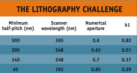
Figure 3. The k1 factor as a metric of the lithography challenge.
While still valid in nanometer technology, Reyleigh’s equation has seen the values for R, k1, and NA change drastically over the last several process nodes (Figure 3). One of the most critical parts of the equation is the value of k1. Implementing a high k1 is easy; implementing a low k1 is hard, and indicates how astutely the lithographer uses the light source.What is noteworthy is that with a k1 lower than 0.5, Resolution Enhancement Technology (RET) is a requirement for anything to print at all.
Lithographers encounter conflicts between design layouts and RET on a daily basis, and long for designers learn more about the new era of lithography. However, the design community, of course, remains blissfully ignorant.
Yet while semiconductor manufacturers have worked diligently to minimize variation through advancements in lithographic equipment and RET techniques, it is necessary for the design community to adopt practices that make designs more insensitive to process variation.
The gap between the lithography and design communities seems to arise because the design rule paradigm for communication between the process world and the design world, which used to work well, can no longer carry enough information to allow the entire system to be optimized. Nevertheless, neither side has yet shown any great willingness to break with the status quo.
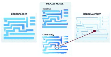
Figure 4. Marginal point detection using the process window model.
A new generation of EDA tools is evolving to fill this gap. It communicates with standard EDA formats, but includes algorithms and simulators tuned to the process requirements of RET. Library generation tools that produce RET-compliant layouts represent one step in this direction. The addition of process simulation to layout verification tools is another. This allows process effects to be automatically predicted and flaws reported as potential design rule violations, using the same interface familiar from normal DRC checks (Figure 4).
As these tools implementing RET compliant knowledge become standardized, the information they require also becomes part of the standard package to be downloaded along with the classical design rules. In this way, the design rule paradigm is not challenged; only the content of the information package has changed. Designers do not need to take seminars on diffraction, and lithographers do not need to learn how to debug RTL. Each group of experts can remain focused on doing what it does best, as long as the tools continue to evolve to fill this gap.
Simple parametric extraction is inadequate
New physical effects and layout complexities result from the combined impact of nanometer scale design and copper process technologies. The proximity of varied design components to one another conspires to make inductance, electro-migration, signal integrity and hierarchical timing analysis critical. In view of these effects, transistors must not be modeled in isolation, but evaluated more accurately across the diffusion characteristics of the entire design.
In metal layers of certain densities, surfaces tend to dish or become convex, changing the resistance and capacitance characteristics of lines. Contacts and vias, which were not points of concern in earlier process technologies, now contribute substantially to total interconnect capacitance. Substrate effects adversely affect on-chip analog functionality, and coupled capacitance is becoming a significant percentage of total interconnect capacitance. Line width variations, and optical and process effects applied post-layout, must also be considered.
Traditional analysis required accurate parasitic information to model resistance, capacitance, coupled capacitance and inductance. The new analysis paradigm requires more. Accurate parasitics must be annotated to accurate geometric information. This means delivering parasitics plus intentional device measurement including X and Y locations, width, length, layer and number of contacts. Current density measurement is necessary to model IR drop and electromigration. This requires a strong link between a robust layout vs. schematic (LVS) tool and a transistor-level parasitic extraction tool.
Non-standard elements, such as handcrafted analog components or MOS devices with irregularly shaped diffusion regions, are more susceptible to current-related issues. The resulting stresses impact electrical behavior, power, and ultimately the lifespan of devices. The only way to accurately assess the stress effect of these components is through post-layout re-simulation, with both parasitic effects and accurately measured physical device parameters. Without a tight link between an LVS tool which can extract all device parameters, and a transistor-level parasitic extraction tool, designs cannot be properly netlisted for re-simulation purposes.
Conclusion
Design for manufacturing in nanometer technologies has the potential to change almost every aspect of the IC design and manufacturing process. It has radically changed the lithographic process in manufacturing, and continues to mold advancements in IC manufacturing equipment and materials. For the design team, it beckons an extensive review of current design practices.
Will concurrent change in both the design and manufacturing disciplines overcome the challenges we face? For those chip design and manufacturing companies who are already on the road to adopting new DFM tools and methodologies, the answer is simple: there is no time to delay.
