A pulsed UWB receiver SoC for insect motion control
The article describes the context and need for embedded operating systems that are more responsive to the power management demands placed on today’s electronic devices. It reviews the design objectives for the two main types of power management, reactive and proactive, and examines how both can be implemented.
For decades, scientists and engineers have been fascinated by cybernetic organisms (more commonly, cyborgs) that fuse artificial and natural systems. Cyborgs allow us to harness biological systems that have been honed by evolutionary forces over millennia to achieve astounding feats. For example, male moths can detect a single pheromone molecule, a sensitivity of roughly 10-21g. Thus, cyborgs can perform tasks at scales and levels of efficiency that would ordinarily seem incomprehensible.
Semiconductor technology is central to realizing this vision, as it offers powerful processing and communication capabilities, as well as low weight, small size and deterministic control. An emerging cyborg application is moth flight control, where electronics and MEMS devices are placed on and within a moth to control its flight direction. Research currently under way is investigating the possibility of mounting sensors on such cyborg insects for their use in the surveillance of hazardous environments. 
To receive commands on the moth, a lightweight, low-power and low-volume receiver (RX) is required. This article describes a pulsed ultra-wideband (UWB) RX SoC designed for the stringent weight, volume and power constraints of the cyborg moth system.
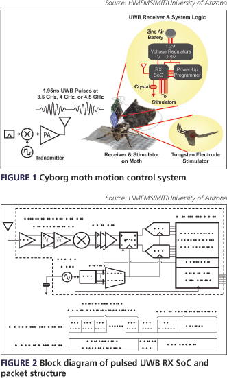
A high-level drawing of the system is presented in Figure 1. Commands are sent from a basestation and received wirelessly on a Manduca sexta hawkmoth. A unidirectional wireless link is employed to reduce power consumption of the moth electronics. A tungsten four-electrode stimulator is implanted in an adult moth to stimulate nervous tissue in the abdominal nerve cord, thereby causing abdominal movements that have been shown to alter flight direction [1]. A 35mAh, 0.2g zinc-air hearing aid battery supplies energy to the system at 1.3V, and is regulated to 1V and 2.5V by a low drop-out regulator (LDO) and a DC-DC boost converter. As the carrying capacity of a moth is limited to approximately 0.8g [2], a highly integrated UWB RX SoC is required. Pulsed UWB wireless signaling is employed as UWB radios can achieve highly integrated, energy-efficient operation in nanometer CMOS processes.
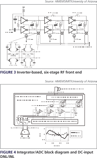
A block diagram of the RX architecture and packet structure is shown in Figure 2. The non-coherent, energy-detection RX receives UWB pulses in one of three 500MHz channels at 3.5, 4.0 and 4.5 GHz. The RX achieves near compliance with the IEEE 802.15.4a standard but with minor changes to reduce power consumption. The received signal is amplified by a low-noise amplifier (LNA) and multi-stage frequency tunable RF amplifier and then squared to baseband.
At baseband, the signal is amplified and then integrated in a 31.2ns window and converted to a 5bit digital code that represents the total energy received within the integration window. An embedded controller triggers the RX to periodically wake up from sleep and look for transmitted data. If a packet is detected, the digital synchronizer determines the timing offset between TX and RX to ±1ns accuracy [3]. A 16-phase delay-locked loop (DLL) provides the necessary clock phase to the windowed integrator and analog-to-digital converter (ADC) to compensate for this offset. The 32MHz system clock is generated by an oscillator and off-chip crystal resonator. Due to the non-coherent RX, no phase-locked loop (PLL) or RF clock is required. Received packets are processed by a pulse-width modulation controller, which drives the implanted electrodes with 2.5V pulses of programmable width, frequency and repetition length. 
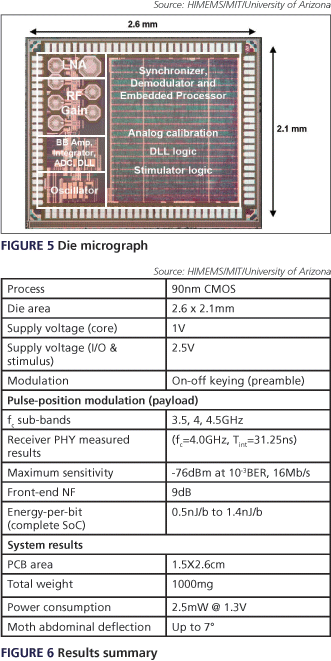
The LNA consists of a common-gate, common-source tuned inverter-based amplifier that realizes single-to-differential conversion, as shown in Figure 3. Following the LNA are five stages of tuned, differential inverter-based RF amplifiers. To achieve gain scalability up to 35dB, a programmable number of amplifiers can be enabled at any time. To DC bias each inverter, the center tap of each stage’s inductor is connected to the center tap of adjacent stages. As these nodes are virtual grounds this technique does not reduce gain. The inverter-based RF amplifier achieves comparable energy efficiency to low-voltage (0.5V) tuned amplifiers [4] while requiring only half the total number of inductors. Moreover, the higher operating voltage allows for a single core supply voltage of 1V while requiring significantly less current, easing power supply demands. Finally, the inverter-based RF amplifiers allow for simple implementation of a squarer with differential outputs.
Following the RF front end and squarer is a three-stage baseband amplifier, an integrator and an ADC (Figure 4). The entire signal chain from LNA output to ADC input is differential to provide rejection of substrate and power supply noise. The integrator consists of a differential transconductor that discharges multiple nodes from the VDD in succession. This pipelined integration approach allows for the use of back-to-back integration windows and provides 2bit of coarse ADC quantization. Due to its dynamic structure, the integrator has guaranteed stability and does not require a high-gain op-amp. Following the multi-stage differential integrator are single-ended flash ADCs that provide 3bit of fine quantization. Set against a 1bit relative compare baseband [4], the 5bit of data provided by the integrator and ADC allow for much faster synchronization and support demodulation of on-off keyed (OOK) signals. At the start of each RX packet, a digital calibration loop determines the appropriate baseband amplifier offset current and integrator current to maximize dynamic range and cancel offsets. The static performance of the 5bit integrator and ADC. A gives a DNL of +0.55/-0.62 and an INL of +1.5/-1.6.
The RX has been mounted on a miniature, 1.2cm x 2.5cm PCB and has successfully received packets on a moth while battery-powered, inducing moth abdominal motion. By changing the pulse frequency, the abdominal deflection can be varied between 0° and 7°. The PCB is attached to the moth’s dorsal thorax with glue and mounted like a fin. As the system weight is slightly more than the moth’s carrying capacity, the moth is not able to gain lift; however, when the moth is tethered from a string, normal wing movement and abdominal response to stimulation pulses are observed. In a separate experiment, mock PCBs have been mounted on a moth’s ventral abdomen using a harness and flight has been demonstrated with a 0.8g dummy load. 
To reduce system weight below 1g, it is necessary to exploit system-in-package technologies that will allow the RX SoC to be stacked with the microcontroller. The stimulator is inserted ventrally at the junction of the thorax and abdomen while the adult moth is anesthetized with ice. Teflon-coated stainless steel wires connect the stimulator with the PCB, looping behind the tip of the abdomen. On power-up, a microcontroller with embedded flash memory programs the RX through a serial interface and then enters a low-power sleep mode.
The RX SoC was fabricated in a 90nm CMOS process. The RX operates at a 16Mb/s instantaneous data rate and achieves a sensitivity of -76dBm at 10-3 BER, corresponding to a duty-cycled sensitivity of -98dBm at 100kb/s. The RX SoC instantaneous power scales from 8 to 22.7mW while demodulating data, yielding 0.5 to 1.4nJ/b. In the cyborg moth system, the duty cycled RX looks for a packet of data every millisecond, requiring an overall average system power of 2.5mW at 1.3V. A die micrograph is shown in Figure 5. Results are summarized in Figure 6.
Acknowledgements
This work is funded by DARPA HI-MEMS program. The authors thank STMicroelectronics for chip fabrication, Goggy Davidowitz, Nathan Ickes, Helen Liang and Parth Sethi for testing assistance, and Tom Daniel and Armin Hinterworth for the Tungsten stimulator.
References
- J. Mavoori, B. Millard, J. Longnion, T. Daniel, C. Diorio, “A Miniature Implantable Computer for Functional Electrical Stimulation and Recording of Neuromuscular Activity,” IEEE International Workshop on Biomedical Circuits and Systems, pp. S1.7.INV 13-16, Dec. 2004.
- P. Mohseni, K. Nagarajan, B. Ziaie, K. Najafi, S. B. Crary, “An Ultralight Biotelemetry Backpack for Recording EMG Signals in Moths,” IEEE Trans. Biomedical Eng., pp. 734-737, June 2001.
- P. P. Mercier, M. Bhardwaj, D. C. Daly, A. P. Chandrakasan, “A 0.55V 16Mb/s 1.6mW Non-Coherent IR-UWB Digital Baseband with ±1ns Synchronization Accuracy,” ISSCC Dig. Tech Papers, Feb. 2009.
- F. S. Lee, A. P. Chandrakasan, “A 2.5nJ/b 0.65V 3-to-5GHz Subbanded UWB Receiver in 90nm CMOS,” ISSCC Dig. Tech Papers, pp. 116-117, Feb. 2007.
Massachusetts Institute of Technology
Department of Electrical Engineering and Computer Science
50 Vassar Street
Cambridge
MA 02139
USA
T: 1 617 253 0016
W: www-mtl.mit.edu
ARL Division of Neurobiology
The University of Arizona
PO Box 210077
Tucson
AZ 85721
T: 1 520 621 6629
W: neurobio.arizona.edu