Sensium: A 1V micropower SoC for vital-sign monitoring
This paper describes the main design components and methodology priorities for development of the Sensium system-on-chip for wireless body sensor networks. The device is targeted at vital-sign monitoring and related medical applications.
The SoC integrates an ultra-low-power wireless ISM band transceiver, hardware MAC, microprocessor, I/O peripherals, memories, 10b delta-sigma, analog-to-digital converter and custom interfaces.
The chip is implemented in 0.13 um CMOS and has a 16 mm2 footprint. It operates from supply voltages as low as 0.9V and is part of a fully disposable body patch for use in ‘last meter’ (also sometimes ‘first meter’) body area networks.
Wireless body sensor networks (WBSN) consist of sensor nodes that are used to monitor vital signs such as temperature, heart rate and electrocardiogram (ECG/EKG). These sensor nodes gather, store and locally process vital signs data, before transmission to a central base-station node. Although prototype modules for such WBSN applications are becoming available, these devices tend to be multi-chip solutions manufactured from off-the-shelf components, and suffer from excessive power consumption and relatively large form factors [1,2].
Improvements to the patient’s quality of care can be achieved through miniaturization and a reduction in power consumption. These objectives dictate the development of a custom system-on-chip (SoC). Although ultra-low-power wireless transceiver ASICs have previously been reported [3-5], this paper describes the integration of a system solution with a full-custom hardware MAC, digital microprocessor core and I/O peripherals, on-chip memory, micropower ADC, wireless transceiver and custom sensor interfaces. This SoC platform device is capable of achieving ubiquitous medical monitoring when interfaced to appropriate body-worn sensors, and represents the state of the art in terms of functionality and ultra-low-power consumption. The encapsulated wireless sensor node is in the form of a thin and flexible patch, comprising sensors, SoC, battery and antenna as shown in Figure 1. The patch is attached to the patient for a period of typically four to seven days, after which it is thrown away and a new patch attached, if necessary.
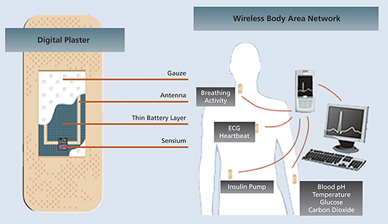
Figure 1. Sensium patch and body area network. Source: Toumaz Technology
The battery is manufactured from environmentally friendly materials such that it can be safely disposed of or recycled. It provides typically 3mAh/cm2 at 1.4V, dropping to 0.9V at end of battery life [6]. The limited energy capacity means that the average current drain must be of the order of microamps to achieve the target operating lifetime. In addition, the battery peak currents must be limited to be no higher than a few milliamps to avoid battery collapse.
These energy constraints require a novel low-power design methodology to be applied at all levels—network protocol, system architecture, circuit topology and implementation—in order to guarantee reliable and robust operation within the battery’s maximum peak current discharge capacity.
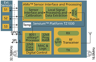
Figure 2. Block diagram of Sensium SoC. Source: Toumaz Technology
Figure 2 shows the SoC block diagram, which comprises three major sections: sensor interface, digital baseband and wireless transceiver. The sensor interface is designed to support a number of different types for monitoring applications including:
- glucose/pH using amperometric sensors;
- motion using a 3-axis accelerometer;
- heart rate/ECG (EKG) using a single lead electrode;
- temperature using thermistors; and
- pressure using a Wheatstone bridge.
A block diagram of the sensor interface circuitry is shown in Figure 3. Mixed signal circuitry provides gain, filtering, biasing and buffering of the sensor inputs. The embedded digital processor may be used for sensor calibration to ensure excellent offset and gain accuracy. A 10b ? analog-to-digital converter samples sensor input signals within a dc to 250 Hz bandwidth. The ADC is a third-order switched op-amp (SO) implementation with a 64 times oversampling ratio [7]. Due to the low frequency nature of the input physiological signals, minimization of dc offsets and 1/f noise is crucial. Optimal switch sizing was key to minimizing 1/f noise while achieving low current consumption.
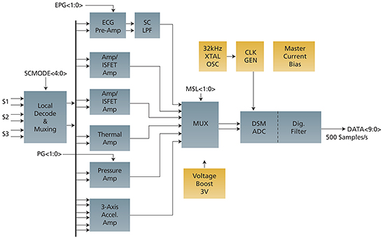
Figure 3. Block diagram of sensor interface. Source: Toumaz Technology
The transceiver is shown in the block diagram in Figure 4 [8]. The receiver uses a two-stage, zero-IF architecture based on a sliding IF approach, which provides advantages in filtering and noise profiling, and thus allows for a lower current consumption than a single-stage direct-conversion architecture.
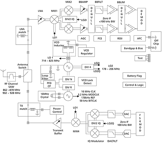
Figure 4. Block diagram of transceiver. Source: Toumaz Technology
The PA stage is designed to deliver -10 dBm into a matched antenna load, giving a range of typically 10m indoors.
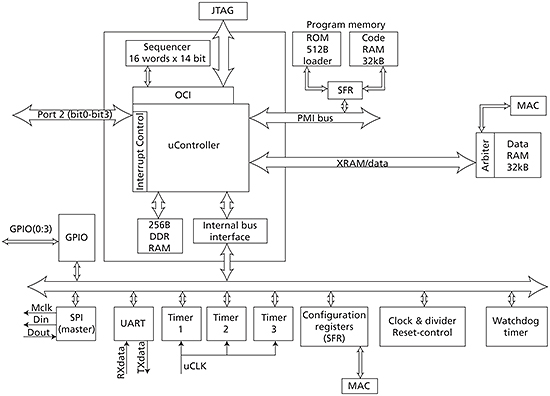
Figure 5. Block diagram of digital section. Source: Toumaz Technology
The digital section contains an 8051 advanced architecture processor, peripherals, memories, timers and the MAC, shown in the block diagram in Figure 5. The MAC protocol block is a custom design to ensure ultra-low-power operation while guaranteeing robust performance, and controls the RF channel selection, listen-before-transmit (LBT) compliance, link establishment, data transfer and sleep management.
The network adopts a master-slave architecture. Unlike traditional peer-to-peer wireless sensor networks, the nodes in this biomedical WBSN are not deployed in an ad hoc fashion. Joining a network is centrally managed and all communications are single-hop.
To reduce energy consumption, all the sensor nodes are in standby or sleep mode until the centrally assigned time slot. Once a node has joined a network, there is no possibility of collision within a cluster as all communication is initiated by the central node and is addressed uniquely to a slave node. To avoid collisions with nearby transmitters, a clear channel assessment algorithm based on standard LBT is used.
To handle time slot overlaps, the novel concept of a wakeup fallback time is introduced [9]. Using single-hop communication and centrally controlled sleep/wakeup times, leads to significant energy reductions for this application compared to more ‘flexible’ network MAC protocols such as Zigbee [10].
A direct memory access (DMA) controller ensures that data samples from the ADC can be continually written to the data memory while at the same time allowing previous data samples to be passed to the microprocessor for processing, or to the MAC for encoding prior to transmission. Up to three independent sensors can be connected to a single SoC, and the sample interval and number of samples per sample time can be independently set for each sensor—this allows sensors with different speed and accuracy requirements (e.g., temperature vs. ECG) to be optimally sampled. These control functions are implemented in hardware, thus in operation the microprocessor core is essentially ‘free’ to run any user-defined application code; for example, fusing data from multiple sensors to allow intelligent decision making.
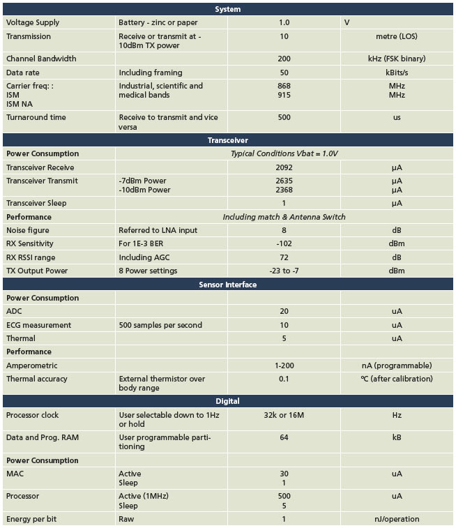
Figure 6. Headline performance parameters of Sensium SoC. Source: Toumaz Technology
The Sensium SoC is implemented in a 0.13 um CMOS technology and occupies an area of 16 mm2. Headline measured performance parameters and power consumption in various operating modes are given in Figure 6. Full functionality for center-processed samples has been verified down to 0.85V; initial yield across corner lots is greater than 95% at a test time of <3s on a Teradyne J750. In WBSN applications this SoC is able to provide typically one to two orders of magnitude lower power consumption than competing solutions, and thus offers the possibility for truly unobtrusive and disposable vital-sign monitoring.
References:
(1) G. Z. Yang, Body Sensor Networks, Springer, London, 2006.
(2) W. Bracke, P. Merken, R. Puers, C. Van Hoof, “A 1 cm3 Modular Autonomous Sensor Node for Physical Activity Monitoring,” Research in Microelectronics and Electronics, pp. 429-432, June 2006.
(3) A.-S. Porret, T. Melly, D. Python, C. C. Enz and E. A. Vittoz, “An Ultra Low-Power UHF Transceiver Integrated in a Standard Digital CMOS Process: Architecture and Receiver,” IEEE J. Solid-State Circuits, vol. 36, pp. 452-466, March 2001.
(4) T. Melly, A.-S. Porret, C. C. Enz and E. A. Vittoz, “An Ultra Low-Power UHF Transceiver Integrated in Standard Digital CMOS Process: Transmitter,” IEEE J. Solid-State Circuits, vol. 36, pp. 467-472, March 2001.
(5) V. Peiris, et al., “A 1 V 433/868MHz 25kb/s-FSK 2kb/s-OOK RF Transceiver SoC in Standard Digital 0.18?m CMOS,” ISSCC Dig. Tech. Papers, pp. 258-259, Feb 2005.
(6) PowerPaper. Accessed on Nov. 18, 2007, <www.powerpaper.com/?categoryId=10625>.
(7) J. Crols, M. S. J. Steyaert, “Switched-Opamp: An Approach to Realize Full CMOS-Switched Capacitor Circuits at Very Low Power Supply Voltages,” IEEE J. Solid-State Circuits, vol. 29, pp. 936-942, Aug. 1994.
(8) A. C. W. Wong, G. Kathiresan, C. K. T. Chan, O. Eljamaly, A. Burdett, “A 1V Wireless Transceiver for an Ultra-Low-Power Wireless SoC for Biomedical Applications,” Proc. ESSIRC, Sept. 2007.
(9) O. C. Omeni, O. Eljamaly, A. Burdett, “Energy Efficient Medium Access Protocol for Wireless Medical Body Area Sensor Networks,” Proc. IEEE-EMBS Symposium on Medical Devices and Biosensors (ISSS-MDBS), pp. 29-32, Aug. 2007.
(10) Zigbee Alliance. Accessed on Nov. 18, 2007, <www.zigbee.org>.
Authors
This paper was written by Alan C-W. Wong, Declan McDonagh, Ganesh Kathiresan, Okundu C. Omeni, Omar El-Jamaly, Thomas C-K. Chan, Paul Paddan, and Alison J. Burdett It is edited from an original version presented at the 2008 International Solid State Circuits Conference.
Toumaz Technology
115 Milton Park, Building 3
Abingdon
Oxfordshire
OX14 4RZ
UK
T: +44 (0)1235 438961
W: www.toumaz.com