Scan infrastructure and environment for enhanced at-speed ATPG
A major issue faced by SoC design teams adopting 90nm and 65nm process nodes is the increase in yield fall-out. At 90nm it is estimated that 30% of yield fall-out is due to performance and signal integrity issues. As a result, accurate and cost effective at-speed manufacturing test and characterization has become evermore critical to achieve high quality silicon.
Traditional at-speed test approaches have proven inaccurate in identifying subtle performance issues This can result in test escapes, overly optimistic device performance characterization, or excessive guard banding leading to reduced performance and yield.
The traditional approach of testing for performance-related defects with ATPG-based solutions has been to generate patterns that target transition delay faults (TDFs). These patterns are typically applied using what is often referred to as ‘broadside’ or ‘double-capture’ timing.
In this technique, shifting of the scan pattern and the launch and capture of the pattern are completely disconnected. Once the pattern is shifted in, two consecutive high-speed clock pulses are used to launch and capture the test pattern. The first clock cycle actually creates the test pattern from the circuit response of the shifted-in pattern. The second clock cycle then captures the response of the created test pattern.
A major drawback of this approach is that the circuit can no longer be treated as purely combinational, as the test patterns result from the response of the functional circuit, which is typically sequential in nature. This therefore results in the need for sequential ATPG. Unfortunately, sequential ATPG is much more CPU intensive than combinational ATPG, often resulting in run-times of days instead of hours, Sequential ATPG also results in reduced TDF coverage. The drop in TDF coverage when changing from single capture to double capture timing is often quite significant.
The sequential nature of double-capture based ATPG also results in a much larger number of test patterns. These pattern volumes can be as much as an order of magnitude greater than the volumes needed for static fault testing. This is very problematic as scan test pattern volumes for static fault testing are already a major concern.
Furthermore, the double-capture technique often results in a lack of at-speed test accuracy. In particular it suffers from a phenomenon known as ‘clock stretching’. This issue is caused by the instantaneous drain on power rails during the launch and capture cycles that results in an increase of the clock period, an overly optimistic performance rating of the device, and reduced delay fault detection.
The BurstMode scan infrastructure
A new methodology has been developed that dramatically improves the results of existing ATPG approaches. The methodology is based on integrating an innovative, hierarchical, at-speed single capture scan infrastructure into the design.

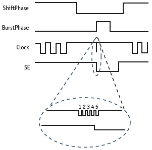
Figure 1. BurstMode timing protocol
Central to this infrastructure is a distributed at-speed timing technology referred to as BurstMode timing. The BurstMode timing technology creates the timing protocol illustrated in Figure 1. During the shift phase, test patterns are scanned in and the results are scanned out at an arbitrary low scan frequency. This allows scan chain segments within different clock domains to be scanned at the same time without any timing complications.
During the burst phase, the scan chains are reconfigured into circular registers and a burst of functional clock cycles is applied while still in scan mode.
Right before the last shift cycle, locally generated scan enable signals are lowered to perform an at-speed single cycle capture.
The burst is long enough to make sure that the supply has time to stabilize before the launch and capture cycles. This eliminates the clock stretching problem experienced with double capture timing. For each clock domain, the clock burst is configurable at run-time to mimic the functional mode of operation from a timing and power point of view. This is essential to catch subtle problems related to crosstalk or IR drop, for example. The alignment of synchronous clock domains is preserved.
This BurstMode scan infrastructure can be used with essentially any ATPG capability. The only requirement is that the test patterns be generated with a pre-rotation, so that after the burst of functional clock cycles the bit values in the scan chains make up the correct test patterns for the targeted faults. This requirement can be met with most commercial ATPG solutions.

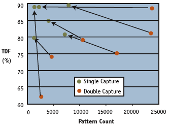
Figure 2. Test efficiency comparison
The single cycle capture approach results in many significant test generation advantages over double capture approaches. The diagram in Figure 2 shows some representative industrial results that highlight the difference in TDF coverage and test pattern count between single capture and double capture timing. The results show that, on average, single capture timing achieves 6% to 7% higher TDF coverage while requiring on average two to three times fewer patterns.
These results become even more dramatic when ATPG compression is used. Compression is directly affected by the number of care (specified) bits in each test pattern, and this number goes up when double capture timing is used due to the sequential nature of the resulting ATPG effort.
The BurstMode scan infrastructure also provides robust timing capabilities that result in further benefits. Paths crossing asynchronous clock domains are handled using a capture-by-domain approach. The transmit and receive flops on the cross domain paths are equipped with additional scan control logic (most of it shared) so that all resulting setup and hold margins on these paths are several (eight or more) shift clock periods long. Multi-cycle and false paths within a clock domain are handled in a similar fashion. In these cases, logic is added to only the source flops of these paths so that they hold their values for the appropriate number of clock cycles.
The net effect of this robust timing control logic is that all paths in the design can be tested at-speed, at the same time. No masking of unknown results from any of these paths is needed. This increased test parallelism and removal of unknown values provides further increases in fault coverage, as well as further decreases in test pattern count and reduction of test generation time. The removal of unknown values also helps to improve fault diagnosis.
Hierarchical scan architecture
The BurstMode scan infrastructure supports a hierarchical architecture to scale with design size, speed and power. A key component of this architecture is the ability to efficiently isolate each core during test application. The core isolation technique uses a combination of existing functional flops (referred to as ‘shared isolation’ flops) and some additional flops (referred to as ‘dedicated isolation’ flops) to separate the design into independent core components, with minimal area overhead and no impact on performance.
Existing functional flops at or near the periphery of the core are used whenever possible to serve as isolation points. Control logic is added to ensure that these flops do not capture data from outside the core during scan testing. Additional flops are sometimes needed to isolate core pins that are not in close proximity to a functional flop.
With this isolation architecture, test pattern generation can be targeted at only the logic within the core, without any need to consider any periphery logic or effects.
A ‘shell’ model is also created for each core that contains any core logic that resides beyond the isolation flops. The shell models are used to create a highly reduced top-level model of the chip so that test patterns can be efficiently generated for any remaining inter-core logic.
There are several advantages to this hierarchical scan infrastructure. Test pattern generation times are reduced, as only individual cores in isolation need to be considered by the ATPG tool. Furthermore, if two or more instances of the same core exist within the design, then patterns do not have to be regenerated for each instance.
This not only saves test generation time but also results in a significant reduction in test pattern volume, as the same core test pattern set can be reused for each instance. For cores used across designs, this provides a complete core handoff capability, including pre-generated and certified test patterns with known fault coverage.
ScanBurst automation flow

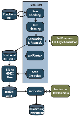
Figure 3. ScanBurst automation flow
A design automation environment compatible with all third-party physical design flows was recently developed by LogicVision to integrate the BurstMode scan infrastructure into any design. The ScanBurst Automation Flow provides a fully integrated set of tools for analyzing a design, creating and integrating a customized hierarchical BurstMode scan infrastructure, and automatically invoking either the FastScan or TestKompress ATPG products. This last step of the flow was developed in collaboration with Mentor Graphics. The fully hierarchical flow is illustrated in Figure 3. All design analysis and IP generation and integration can be performed at either the RTL or gate levels. The design analysis includes such things as the identification of shared isolation flop candidates, as well as the identification of transmit and receive flops on clock domain boundaries.
The integrated IP includes both the BurstMode control logic, as well as (optionally) the TestKompress Embedded Deterministic Test logic.
Scan chain stitching and optimization is performed post synthesis. This step is tightly integrated to all major third-party physical design flows including RTL-to-GDSII flows and has no impact on design performance.
Once the scan infrastructure is integrated, either the FastScan or TestKompress ATPG tool is invoked to perform fault simulation and create all manufacturing test patterns.
LogicVision
25 Metro Drive,
Third Floor
San Jose,
CA 95110
USA
T: +1 408 453 0146
W: www.logicvision.com