Re-evaluating the flow for package-aware chip design
Chip and package design are all too often still seen as separate stages in the design process. In today’s nanometer age and with the growing use of techniques such as system-in-package, this lack of integration can have catastrophic results. Package designers frequently encounter overly complex and un-routable silicon that requires multiple iterations to fix. Problems that occur so late in the design flow have an inevitable impact on both NREs and time-to-market.
The article describes an alternative methodology, ‘package-aware chip design’, that allows various I/O and related challenges to be addressed early in a project’s life with the goal of creating a one-pass flow. This methodology needs to be applied ideally during prototyping and certainly before floorplanning. The objective is give both chip and package engineers a clear view of the challenges that lie ahead.
Specific requirements for this methodology are discussed. The author explains why and how it enables a die to be designed within the context of the external environment, the package substrate and the PCB. He highlights the development of design constraints at the appropriate design stage to ensure the best placement of I/Os, associated logic, bumps and routing and the best interplay between various design disciplines.
Progressively smaller process geometries have long meant higher performing integrated circuits (ICs) with higher levels of functionality. But in the nanometer era, they have also meant skyrocketing design and fabrication costs to deliver chips that boast a greater numbers of pins, more I/Os at accelerated speeds and mixed analog and digital technologies. There are also more power distribution challenges, others posed by higher frequencies, more demands on power plane integrity, and simultaneous switching output (SSO) issues.
Meanwhile, the growing influence of consumer electronics (CE) has greatly increased market pressures, requiring designers to do more with less. The headlong rush to miniaturization to cater to the needs of the CE sector has created a need to cram more chips into a single package and to do so cost effectively. This has led to innovations such as the system-in-package (SiP), 3D packaging with stacked dies, and 3D transistors to serve as alternatives to single-die systems-on-chip (SoCs).
This latter trend implies that an effective design flow should incorporate design optimizations and tradeoffs done in different environments that pay ongoing regard to how a signal propagates through the die, the package substrate and ultimately the printed circuit board (PCB). After all, companies do sell finished devices, not bare silicon.
However, most chip-level I/O planning is still done in isolation from the design of the package or the rest of the system, leading all too often to overly complex and un-routable silicon that requires multiple iterations to fix at a very late stage in the game. As more functionality is added to silicon, consequently higher I/O counts running at higher speeds and operating at lower voltages will only exacerbate this problem.
There are also the increasing demands being placed on package design to play its role in ensuring that performance requirements are met, that balanced power is provided for the chip, and that all this is achieved within predefined (and extremely tight) cost margins. While many chip designers may still assume that the package is the package engineer’s problem and that they require little insight into the rest of the system, it is becoming increasingly obvious that traditional perspectives and a rigid adherence to perceived job responsibilities will no longer serve. A new approach is required, one that is both package– and system-aware and which enables – as much as is possible – the concurrent design of chips, packages and systems.
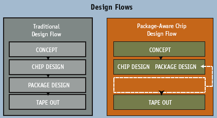
Figure 1. Employing a package-aware chip design methodology simplifies and optimizes IC and package design. It enables early prototypes and automates manual efforts with fewer iterations.
Towards this goal, a methodology often referred to as ‘packageaware chip design’ is emerging. It can already be deployed during prototyping, implementation and verification and enables chip designers to take package routability, power delivery and I/O behavior into consideration during the initial I/O planning process. This holistic approach to chip design, addressing the impact of package parasitics on interconnect performance, ensures that due consideration is given to all relevant elements in the design optimization process. In particular, electrical performance can be understood and addressed before final implementation.
This new method also includes interconnect synthesis processes where the cross domain interconnect – chip/package and PCB – is considered as a whole during I/O planning and sequencing. Package-aware I/O planning, with I/O synthesis, placement and routing capabilities, is useful for flip-chip implementations. I/O synthesis creates an optimized I/O plan along with cost-effective packaging options, satisfying physical and electrical constraints.
Package-aware I/O planning
Package-aware chip design should ideally begin early in the prototype phase and before floorplanning. At this point in the design flow, tradeoffs can most effectively be made and the team can settle on a ‘known good’ I/O plan that is routable in the package and within cost targets.
Having an I/O and package plan early in the project’s life gives chip designers a means by which to analyze the interconnect from the chip’s I/O buffers to the PCB. The resulting timing and signal integrity (SI) data can then help to define design constraints.
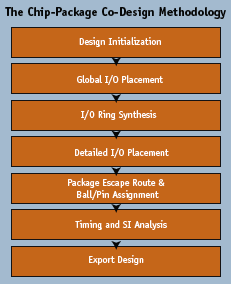
Figure 2. Chip/package exploration during early planning enables trade-offs with minimal impact. Optimizing the die and package leads to overall cost savings.
Realistic constraints will in turn further ensure that the final design is routable, keeps to budget and has a shorter design cycle. Other benefits can include minimized die size as a result of optimized I/O and bump placement, and the generation of data that can be used to inform the most cost-effective choice of package.
Armed at an early stage with details of the package I/O assignments, the package engineer can draw up his/her initial layout or implementation. Both the chip and package design flows can now proceed forward as parts of a unified entity rather than as completely separate designs. I/O planning, as part of this methodology, offers a transition from a traditional, sequential flow for chip and then package design to one that is concurrent. The result is a ‘one pass’ design flow where multiple iterations are avoided. I/O planning includes synthesis, placement and routing.
Synthesis and placement begin the process with the creation of a correct-by-design I/O ring that satisfies the appropriate set of constraints: e.g., signal/power/ground (SPG) requirements, package design rules, the core floorplan and board-level I/O requirements.
Synthesis must here take account of the signal- and powerintegrity factors that will ensure the design meets SPG requirements, including the power and ground needs of the I/O drivers. First, synthesis calculates current requirements of a particular voltage plane based on driver models, then it calculates the number of balls needed to meet those requirements. Where there are multiple voltage domains, synthesis must accommodate each power domain.
The synthesis engine must be able to optimize the I/O ring plan for minimum die size and I/O row area. If the die size is fixed, the synthesis algorithm will succeed only if a feasible I/O ring plan exists for the given die size.
The placement engine positions I/Os, bumps or bond pads, and pins. Prior to synthesis, it estimates I/O cell placement around the periphery of the die. This process must take account of certain requirements: e.g., pre-placed instances (I/O and/or core), groupings of I/O cells (such as bus I/Os), and electrical constraints. Once the I/O ring has been synthesized, the placement tool can then generate a legal I/O placement.
This package-aware methodology can be used across various designs. It can feature on small analog/mixed-signal projects where rules-based I/O sequencing is more critical and pad-limited designs are common. It can be used for SiPs where chip-to-chip I/O planning must be coordinated simultaneously across multiple chips and the substrate. Or, it might be employed for high I/O count flip-chip devices where package costs can become prohibitive unless there is an intelligent I/O planning methodology. The package-aware strategy has its part to play in projects ranging from the simple to the highly complex.
There are many challenges in implementing this methodology and they cross various disciplines. But the foremost requirement is a single, unified data model that can support both the chip and the package as active components in a single user interface. This model allows engineers to explore trade-offs on both the chip and package via metrics that are immediately fed back to the design team, and which contain a complete understanding of both the electrical and the physical constraints for the chip and the package. The data model facilitates the optimization process by bringing all design elements into the synthesis flow, using the industry-standard OpenAccess database. Lastly, it serves as the repository for a ‘golden’ chip/package interconnect matrix because it is where both chip and package connectivity can be managed in their entirety.
The package-aware methodology also needs to be able to function within existing design flows. Therefore, it supports industry-standard formats such as LEF/DEF on the chip side and APD on the package side. Because signal and power integrity are critical to the success of any packaged chip, the methodology’s accompanying software must have the ability to evaluate electrical performance as part of the prototype flow.
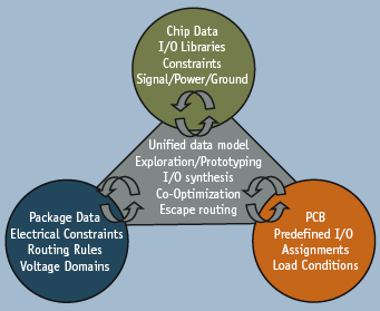
Figure 3. The unified data model is used for exploring tradeoffs on the chip and package with an immediate feedback metric.
The software linked to this methodology will operate in a planning environment where all data may not be present and the design would be incomplete. As a result, verification –– or extraction and analysis –– tools must be flexible and smart enough to account for these limitations, while providing results that are nevertheless accurate enough to be useful. Additionally, the package-level routing and voltage-domain plane-cutting needs to be design rule check (DRC) clean and abide by packaging rules. This is important when establishing valid chip-to-package net assignments and proper power plane bump/ball assignments.
Early extraction and analysis is used for initial parasitics information about the die and package nets, though final signoff accuracy requires a 3D field solver. In the early stages of the design, PCB traces can be represented as distributed resistance, inductance, capacitance (RLC) circuits with standard termination. Using this data, delay engines can calculate timing effects due to resistance, capacitance, inductance, conductance and crosstalk, and should be able to calculate the delays from individual nets or groups of nets. These engines also determine timing skew for differential pairs, clock switches and data/clock nets.
A signal-integrity engine supplies crosstalk data for delay analysis and noise estimation. Through the use of extracted package parasitics and IBIS driver models, it helps optimize the I/O plan in synthesis. Then, a power-integrity engine analyzes voltage and current values on power nets, while frequency-domain analysis determines de-coupling strategies.
Conclusion
A new approach to IC design that is package and system aware is required. Floorplanning of the chip and placement of IOs cannot be done in isolation and a comprehensive approach that enables a concurrent design methodology for chip and package is a must.
What is needed is a means to address the problem by allowing the die to be designed within the context of the external environment –– that is, the package substrate and the PCB. It should be able to accept various constraints from diverse design domains including PCB, package and IC. It should be able to produce optimal placement of IOs, associated logic, bumps and routing on the top layer from IOs to bumps. A capability is needed to synthesize the bump patterns to achieve timing closure, signalintegrity requirements, and escape in the given package substrate layers along with exploration capabilities.
Developing such a solution for full chip integration early in the design and being able to simultaneously visualize the chip in the package ensures design convergence. It would give chip designers iteration-free verification when the design is done and eliminates the ad-hoc approach to chip-package design.
In conclusion, a more holistic approach to system interconnect through the adoption of a package-aware chip design methodology enables chip designers to make better decisions based on empirical data rather than by ‘rule-of-thumb’ schemes used today. It encompasses prototyping, implementation and verification, the three phases of a chip design flow that will fully enable package-aware chip design.
Rio Design Automation
2901 Tasman Drive
Suite 112
Santa Clara
CA 95054
USA
T: +1 408 844 8038
W: www.rio-da.com