Left shifting DFM analysis into the PCB design flow
What do we mean by a ‘left shift’ in design for manufacturing (DFM) analysis? Think of it as moving the DFM analysis from a tool run by the manufacturer into an integrated solution within the printed circuit board (PCB) design system. It is a major advance in the design of PCBs, allowing users to ultimately eliminate many of the iterations used for DFM analysis today, thus making the overall flow more efficient.
There are several different ways of shifting DFM analysis into the design system. A minor one is to develop processes that perform manufacturing analysis in-house; a major one is to apply DFM analysis within the design system using a correct-by-construction methodology. In general terms, each time the analysis is more closely integrated with the PCB design system, the overall design process improves, although the greater the degree of the shift applied, the greater the benefit.
Traditional design analysis
Let’s first look at the typical iterative approach to DFM analysis for PCBs today. Traditionally, a designer will use some simplistic analysis within the PCB design system, but will then rely on the manufacturer to apply external tools to the analysis of a set of output files. In this external, post-design processing environment, any manufacturing problems that are detected must be manually passed back from the manufacturer to the designer for fixing. This inevitably leads to iterations late in the design process when it is expensive to update a nearly completed projected. Worse still, once the first set of changes are made to resolve manufacturing problems found during analysis, a new set of manufacturing data must be produced and the cycle starts over again. The efficiency of this iterative approach varies depending on the cycle time, the level of integration between the DFM tools and the design system, and the difficulty any necessary changes may entail at such a late stage.
Moving DFM analysis in-house
External manufacturing analysis typically has problems with extended cycle times, conflicting priorities, difficult communication and difficulties making changes to nearly completed designs. This, in itself, makes for a slow iterative cycle. So why not shift that analysis in-house to where the PCB design is carried out?
By making DFM analysis an in-house process, the cycle time is no longer subject to outside influence from the manufacturer. The process of generating manufacturing analysis results is directly controlled by the designer as part of the design process. This improves the cycle times needed to iterate through the process of resolving manufacturing violations.
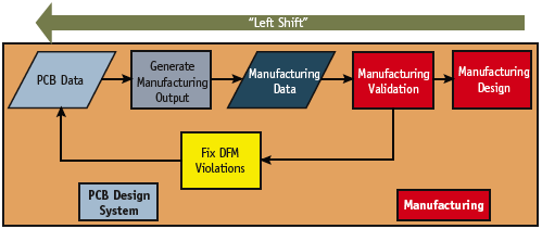
Figure 1. Typical iterative DFM Flow using integrated PCB and DFM solution.
Running the analysis externally can also frequently lead to problems and delays because the design house and manufacturer have conflicting priorities. For example, the manufacturer will probably have multiple customers, each with their own unique requirements. This can make it hard to ensure that the manufacturer gives your particular design the immediate attention required to meet today’s time-to-market requirements. By bringing the analysis in-house, you can determine your own ranking of priorities.
Communication is difficult when dealing with two independent systems, and this is only made more challenging when these systems are run by different companies. The difficulty here lies in communicating the details of any manufacturing problems in such a way that they can be resolved in the PCB design system. By running the manufacturing analysis in-house, designers can work directly with the person running that analysis and ensure that issues are clearly identified and resolved within the terms of the core design system.
Once you have the results of the DFM analysis, it can be difficult to resolve those issues in a nearly completed design. The closer that the analysis is to the designer, the more often it will be run, and hopefully the easier it will be to uncover and fix violations sooner in the design process. Again, an ability to run DFM analysis early in the design flow – or whenever the designer deems most appropriate – is a procedural change that can best be made if that process is being run internally.
However, simply bringing DFM within the design house does not solve the major problems that currently arise if two different systems are still used to do design and DFM checks. Any process that involves two systems adds complexity and inefficiencies to the development of PCBs and inevitably leads to some manifestation of those same problems of lengthy cycle times, communication errors, and the headaches that occur when trying to fix violations that are found near the design’s completion.
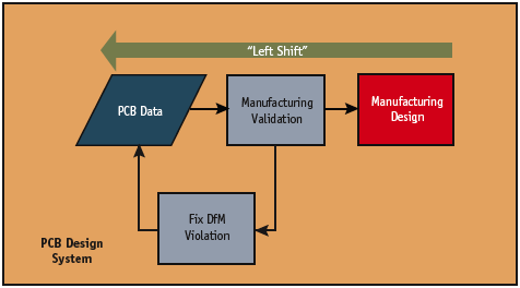
Figure 2. DFM Flow using integrated PCB and DFM solution.
Integrating DFM into the design system
So, using two non-integrated tools for PCB design and then manufacturing analysis can lead to inefficiency within the design process. By contrast, Figure 2 shows how the overall design process can be improved by using an integrated solution.
On one level, by shifting the DFM process into the design system, a designer can take full advantage of a complete array of manufacturing analyses that would not normally be addressed by his design tools.
Cycle times can be greatly reduced by allowing the designer to run the manufacturing analysis within the design process. Since the analysis can be run without having to generate manufacturing output files, and the violations can be reviewed natively within the design system, the overall process of fixing any problems is much improved. By removing the need for a great deal of person-to-person communication, issues can be easily understood and fixed within the design flow.
When DFM analysis is available to the designer, it can also be run at strategic times within the design flow. This direct relationship between the engineer and the analysis means that the critical decision as to when it is best to run the DFM checks is defined by the company doing the design. There is no need to interface with external suppliers that might make such judgments based on conflicting priorities. This approach also allows the analysis to be run early in the design process instead of on a nearly completed design.
However, one further shift can be enacted to allow the designer to use a correct-by-construction methodology using DFM rules while actively designing the PCB. A correct-by-construction strategy eliminates the traditional and iterative process of design-then-check-then-design for DFM and instead allows manufacturing rules to be applied dynamically during layout.
Dynamic correct-by-construction online DFM analysis
As discussed above, there are different ways to left shift the DFM analysis into the design process. First, it is shifted from being run at the manufacturer to being run at the same location as the design is being completed. Second, it is shifted when it becomes an integrated part of the design process although it remains a separate post-design process. The final shift further improves efficiency by integrating the analysis into the design system as an online view of manufacturing violations with integrated correct-by-construction processes. Figure 3 shows this type of dynamic manufacturing analysis integrated as part of the full PCB design system. Here, one of the most effective ways to reduce development costs and improve time-to-market is to use a correct-by-construction methodology as part of the design process. This eliminates expensive design iterations and leads to a huge overall improvement in the effectiveness of the PCB design flow.
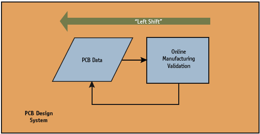
Figure 3. Correct-by-construction DFM Flow within PCB design system.
As the analysis left shifts from being an external application to becoming a dynamic function of the design system, a simplification of the usage flow can be seen. It creates a mechanism that allows companies to easily incorporate manufacturing analysis with minimal effect on the overall design process. All of the inefficiencies that we have seen associated with DFM analysis are resolved when the analysis becomes integrated as correct-by-construction into the design system. Let’s consider the kind of usage flow we are discussing here in more detail.
The flexibility of rules
The first thing about defining a correct-by-construction method for DFM analysis within a PCB design system is to define the particular rules and types of rule that need to be followed during the design process, with some regard to the points at which they are applied. These rules are similar to those used in post-design analysis. However, because we are working within a correct-by-construction methodology, some ‘hard’ rules are required. At the same time, the designer also needs these to be process-tolerant rules that meet the manufacturing requirements, but which do not overly constrain the system so that the design is difficult to complete. The goal is to define rules that allow the design to be manufactured anywhere with confidence. Once the DFM rules have been defined, the design system needs to apply them in such a way that they aid the designer during layout, and do not interfere with the basic process. For example, design for assembly (DFA) rules need to be applied during placement to ensure that components are placed with due regard to the soldering and assembly processes. However, these rules should not be such that they remove the designer’s ability to temporarily place parts in violation to the DFA rules. The design system needs to support a combination of correct-by-construction techniques, dynamic rules checking, and permissions for temporary violations that can be fixed later.
Design for fabrication (DFF) needs its own set of rules that are definable by the designer for the analysis of acute angles, slivers, solder bridging, thermal dissipation, exposed metal, and more besides. They are defined in a similar way to how rules are created for DFM post-analysis checking, but also require some hard definition that is followed during layout. Therefore, during interactive and automatic routing, these rules are followed as hard, correct-by-construction rules, with the caveat that there may be cases where the designer determines they are ‘preferences’. Again, we are allowing for temporary violations that will be resolved later on in the design flow.
Once the DFM rules are represented in the design system, they can be used as part of the base set of constraints that includes net clearances and electrical rules. It should be up to the designer which of these manufacturing rules are used for correct-by-construction and which are defined as ‘preferences’.
The application of DFM dynamic analysis has many advantages as part of the design system layout process. It is always more efficient to apply a set of rules to be used during the design process than to try to process rules into a design after the fact. Simply making the manufacturing rule violations more dynamic, where the designer no longer has to run a post-processing step, delivers a substantial increase in efficiency.
The secret to an effective correct-by-construction methodology is that the design system has the ability to apply the manufacturing rules without making the overall design process more difficult. Therefore, these rules need to be a designer-controlled combination of hard rules to be followed and optional rules that are used as a preference. Flexibility is key.
Conclusion
Each time a left shift in the manufacturing analysis is applied to the PCB layout process, there is a gain in efficiency. The alleviation of multiple iterations between the board designer and manufacturer, as well as the deployment of manufacturing rules early in the PCB layout process, can positively influence the overall costs of the design. The left shift results in increased board yields generated during manufacturing and a reduction in overall cycle time to complete a design. The final goal of a left shift program is to allow the design system to support a correct-by-construction methodology using the DFM rules to eliminate costly post-design iterations. The ultimate success of this approach is the development of a PCB design flow with highly integrated manufacturing analysis that assists the designer in the completion of the task while that analysis remains transparent to the overall layout process.
Mentor Graphics
Corporate Office
8005 SW Boeckman Rd
Wilsonville
OR 97070
USA
T: +1 800 547 3000
W: http://www.mentor.com/
