Leakage power optimization for a wireless comms SoC
Leakage has become a critical concern for sub-100nm silicon process technologies. It had started to become a significant factor in a chip’s overall power profile at 130nm, but by 90nm things had worsened with leakage accounting for perhaps 30% of a chip’s total power consumption. At 65nm, leakage represents more than 50% of power consumption.
Similarly, the dynamics of yield have changed. Before the 100nm threshold was crossed, defect-related failures accounted for the majority of chip failures. However, at 65nm, parametric failures – i.e., chips that fail to meet power and timing specifications – have become dominant.
Because of these recent developments, chip designers at both integrated device manufacturers and fabless semiconductor companies are searching for new ways to control leakage power and leakage variability, and to substantially increase parametric yield.
This article shows how Blaze has been working with one semiconductor company to address the issue of leakage power.

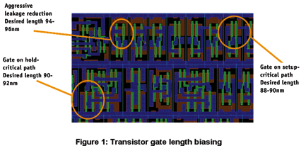
Figure 1. Transistor gate length biasing
Transistor biasing
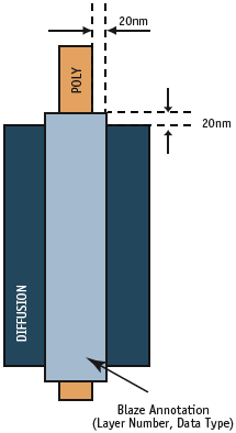
The client’s chip designers were interested in Blaze’s approach because it was different from anything they had ever seen before. The Blaze MO tool suite optimizes a design for leakage power through a combination of techniques. It biases individual transistor lengths based on power and timing requirements. Hold-critical transistors are positively biased (lengthened by a few nanometers) making them a bit slower, but less leaky. Non-timing-critical transistors are positively biased aggressively to reduce leakage current even further. Setup-critical transistors are not biased. Figure 1 illustrates this approach. However, the tool does not actually change the layout of the transistor gates. Instead, it adds an annotation layer to the GDSII file. The shapes on this annotation layer define displacements of the target edges that the OPC tool seeks to hit. For example, by shifting the target edges of a 90nm transistor gate outward by 1nm per edge, Blaze MO induces model-based OPC to create a mask design that will print a 92nm gate (Figure 2, p30). Although the annotation shape is much longer than the transistor gate, the actual amount of the biasing is only a few nanometers. There are attributes associated with each shape that instruct the OPC tool by how much to bias the transistor gate.
Another method of reducing leakage power is to dynamically assign the threshold voltage (Vt) of individual cells based on power and timing requirements. Setup-critical cells are swapped out and replaced with lower Vt cells; hold-critical and non-timing-critical cells are swapped out for higher Vt cells.
Setting the foundations
As with any new technology, some setup work is required. In our case, this preparation needs to take place in both the library development and the manufacturing groups. This preparatory work only needs to be undertaken once for each process technology. It does not have to be repeated for each individual design.

Figure 2. Blaze annotation
Library development group
The tool requires a number of variants for each library cell. These variants reflect the results of the transistor gate-length biasing and are used to verify that the timing integrity of the chip has been preserved. After the Blaze optimization is complete, the Verilog netlist is updated by swapping in the variant cells and the new netlist is used to verify timing correctness. It took the client’s library development group, working together with Blaze engineers, about four weeks to develop, verify, and characterize the required variants. Since this was the first time that this type of preparatory work had been undertaken, both Blaze and the manufacturer believe that this time can be greatly shortened in future. Indeed, having established the flow, they expect that it will take about one week to prepare subsequent variant libraries.
Manufacturing group
The preparatory work required of the manufacturing team involves updating the OPC scripts so that they recognize the Blaze annotation layer and act accordingly. The shapes on the annotation layer in the GDSII file instruct the OPC tools how to bias each transistor according to pre-defined directives.
With this client, Blaze provided some simple examples of how to modify the scripts for the two most popular commercial OPC tools. Blaze also provided a verification layout (automatically constructed using the design rule guidelines) and has internal utilities to validate the post-OPC litho-simulation result. Based on our experiences with this implementation of the tools, the whole process should typically take a few days.
Initial test vehicle
After detailed technical discussions, the client’s design team agreed to run a test design through the Blaze MO optimization. They chose a processor core that they claimed had already been optimized for leakage using all the techniques previously at their disposal. They said that it was so highly optimized that they would be surprised if the tool could reduce leakage by 5%.
After the preparatory work was completed, the designers delivered the original hardened core to Blaze. It contained about 100K cell instances of which 80% were optimizable combinational cells. After evaluating the design, Blaze engineers decided to perform the optimization in two separate steps. First, they performed positive transistor gate length biasing on the combinational logic. After that, they performed the Vt assignment and swapped out low Vt cells for higher Vt cells to reduce leakage.
It took about four weeks for the Blaze engineers to familiarize themselves with the design flow, run the first set of optimizations (the gate length biasing and the Vt assignment) and perform the timing signoff and physical verification. Again, as this was the first time Blaze optimization had been performed in this environment, it took longer than it would in a mature flow. It would normally take just a few hours to optimize a design of this size. The application of Blaze MO transistor gate length biasing reduced the leakage by 15% in the combinational cells and by 10% for the full block. Then, the Vt assignment was performed without transistor biasing and leakage was reduced by 30% in the combinational logic and 20% for the full block. Finally, the design was optimized using both gate length biasing and Vt assignment. The leakage reduction was 40% in the combination logic and 25% for the full core.
As mentioned above, the designers had previously stated that a 5% reduction in leakage power would justify further investigation. A reduction of 25% greatly exceeded their most optimistic expectations.
Full-chip implementation
Based on the results for the processor core, the design team gave Blaze the go-ahead to optimize the entire chip, a wireless communications SoC implemented in a 90nm multiple-Vt, low-power process. It contained two instances of the processor core (2 x 100,000 cells), a DSP block (200,000 cells) and about 1.6m top-level cells – a total of about 2m cells. The computing environment included high-performance 64-bit Linux servers, each configured with 32-64GB of RAM. A full-chip Blaze optimization consumed about 25GB of RAM and ran overnight.
The designers had first taped out the design several months earlier. They extrapolated the results from the initial test design and based on the amount of combinational logic in the chip, they estimated that full-chip leakage could be reduced by 15%. Blaze MO was only used on combinational logic. It was not allowed to touch clock trees, sequential logic, memories, analog circuitry, or I/O cells.
When operating on an entire chip, the Blaze optimization can be performed hierarchically. For this design, the processor core was optimized once and instantiated twice. The DSP was also optimized at the block level. The remainder of the logic was optimized at the chip level.
After the optimization is complete, the design must be verified through the golden timing and signal integrity signoff flows. If any problems are detected in the optimized design, the tool must repair that part of the chip by backing out some of the optimizations. It took about four weeks to optimize the design and perform timing, SI and physical verification. In terms of leakage, the design team was able to reduce full-chip leakage a few percentage points by using some of their own techniques. With the Blaze optimization, the full-chip leakage reduction exceeded their projection of 15% versus the original design that they had taped out in March.
After applying some last-minute ECOs, the final design was re-optimized using Blaze MO’s incremental ECO optimization capability. As a final verification step, DRC/LVS was performed and then compared to the original pre-Blaze design. The only differences between the two should have been the annotation layer and the higher Vt cells that had been swapped in, and that indeed was the case.
The chip was taped out two months after the first optimized design. As mentioned above, it took about four weeks to perform the Blaze optimization. However, working hierarchically, some of this work was done in parallel with physical verification. With some additional fine-tuning to the flow, the Blaze optimization should be achievable in less than two weeks. On a hierarchical design, Blaze MO does not add any wall-clock time to the closure of the blocks. However, the top-level optimization does add a few days to the tapeout schedule.
Client’s confidence
Based on these results, the client’s design team has committed the Blaze-optimized design to silicon and plans to use the tools on another design, this time for a 65nm chip. The leakage improvements, as a percentage of total power consumption, at 65nm are projected to be even greater than at 90nm.
Conclusions
Leakage power, and the associated impact on parametric yield, has been identified as perhaps the most critical issue facing designers of sub-100nm chips. Chip designers today face challenges that did not exist as recently as two process generations ago. Even on designs that have already been optimized for leakage power, a combination of gate length biasing and Vt assignment can deliver results that cannot be attained using other methods.
Blaze DFM
1275 Orleans Drive
Sunnyvale
CA 94089
USA
T: 1-408-542-8020
F: 1-408-542-8021
W: www.blaze-dfm.com