Inexact computing means knowing exactly what to cut
Pruning back circuits can boost performance for some applications.
‘Inexact computing’ may sound like a contradiction in terms—or an all-too-frequent occurrence—but the technique is gathering increasing interest in the post-Moore’s Law era.
The technique is a response to increasing process variation coupled with demands for low-energy consumption. As opposed to an ‘exact’ computing model, an inexact approach exploits the fact that there are some applications where the engineer can trade off the accuracy of a circuit’s output against a need to comply with less than 100% with the specified result, and thereby greatly reduce energy needs.
A surprising number of end-uses fit this model, though they do vary in terms of their tolerance for inaccuracy. They can be found in areas such as embedded computing, multimedia and mobile communications. Specific instances include hearing aids and digital cameras.
To date, inexact designs have typically used voltage scaling. But the techniques involved can create their own overhead. Similarly, it might not always be possible to precisely tune the supply voltage as needed when the application is running.
At this year’s Design Automation and Test in Europe conference, a U.S.-Swiss-Singaporean team put forward an alternative approach that is essentially based on identifying and then cutting away those parts of a design that are not entirely necessary. The team calls its approach ‘Probabilistic pruning’.
“Our initial tests indicated that the pruned circuits will be at least two times faster, consume about half the energy and take up about half the space of the traditional circuits,” said Avinash Lingamneni, a Rice University graduate student who presented the research at DATE on behalf of his own school, Singapore’s Nanyang Technological University (NTU) and the Center for Electronics and Microtechnology (CSEM), a Swiss research institute.
The pruning is achieved by first identifying how much error an application can tolerate. To get some context as to what this means, Christian Enz, CSEM’s lead for the project, said, “We know that many perceptive types of tasks found in vision or hearing applications can easily tolerate error magnitudes of up to 10%.”
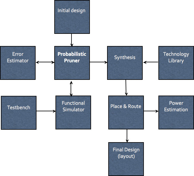
The next step is to estimate the probability that a circuit within a design will be active, prune away those with the lowest metrics, compute the resulting error in the circuit and check this against the target tolerance. A clearer idea of this process can be gained from the flowchart shown as Figure 1.
The Rice-NTU-CSEM group has then gone a step further by integrating their pruner into a logic synthesis EDA flow using tools supplied by leading vendors, including ModelSim. This is shown in Figure 2.
In addition, two approaches to the trimming can be taken. Uniform probabilistic pruning (UPP) is used on applications that require uniform circuits. Weighted probabilistic pruning (WPP) is applied to those where weights are associated with the output of various circuits.
Test chips were developed by printing pruned and unpruned circuits side-by-side on the same silicon for the 180nm (low power) and 65nm (high threshold voltage) technologies at foundry TSMC, and the 90nm (normal threshold voltage) technology at IBM.
In achieving the gains cited above, the team offered five other takeaways from its work.
- Gains obtained for applications that could use a WPP strategy were higher than those that required UPP, although improvements in both were achieved.
- There were also “more significant gains” for parallel circuits, which provided a large number of paths to prune than for serial circuits, which offered far fewer.
- The gains achieved through pruning were proportional to the ratio of circuits pruned to the original design, and “largely independent” of process technology, depending more on logic synthesis constraints.
- Error in a pruned circuit was independent of variation in parameters such as the drain voltage, unlike other inexact design strategies.
- Error does currently rise sharply beyond a critical amount of pruning, much as it does for so-called ‘critical voltage scaling’ points, although this should be fixed by adding a parameter variation element to the process.
“We believe to have convincingly shown through extensive simulations that our technique achieves significantly better savings along all three [major] dimensions—energy, delay and area—while having comparable error, over the conventional scaling schemes,” said the group’s DATE presentation.
“Other benefits include the lack of dependence of the amount of error on any particular process technology and faster design time than conventional voltage scaling schemes as a result of easy integration into a logic synthesis-based CAD flow.”
The next step for the research is to develop a complete prototype chip for a specific application, most likely a hearing aid.


The text for this article seems to be wrong, it’s referencing a different subject (a different article)?
Thank you, this has been corrected.