High quality scan test with minimal pins
Changes in defect distribution, increasing design complexity and pressures from the specialist I/O and packaging arenas are creating a dilemma during component test. On the one hand, the generation of more test patterns would appear to be necessary; but on the other, fewer test ports are available.
The article describes a strategy for addressing this tension by the appropriate augmentation of scan compression technologies with techniques that minimize the number of test interfaces required and enable reduced pin-count test (RPCT). These can meet demands for high-quality test without increasing cost or adding unacceptably to design times. The article also addresses how low pin-count test methods support modern design realities such as multi-site test and volume diagnostics.
Scan testing is the primary method used to detect defects in most digital devices. Changes in defect distributions and quality demands are demanding more and more test patterns, while packaging and pin limitations are creating a need for smaller test ports. Embedded compression technologies can be used to support these conflicting requirements with minimal impact on cost.
Keeping pace with complexity
Scan technology uses special digital flip-flops (DFFs) or latches, called scan cells, that can be controlled or observed from a tester. These scan cells operate as normal DFFs/latches in functional mode but can be configured and daisy-chained into several shift registers during test mode. These are called scan chains. Because scan chains can control or observe the sequential logic in a circuit, the complexity of a design can be broken into combinational logic blocks among controllable/observable scan cells. The algorithmic challenge of making test patterns is greatly simplified and can be supported by automatic test pattern generation (ATPG) tools.
Scan patterns are structural patterns, in that they validate the correct operation of the logic gates. For many years, static scan ‘stuck-at’ testing was the main method used for digital devices. On higher performance devices, test engineers would also apply a functional pattern set to validate that the device functioned at the operational frequency.
Recent advances in silicon fabrication processes have enabled device integration and a steady increase in gate count. These process changes are causing variation in defect distributions. In response, our approach to test has needed to change. The growth in gate count correlates to an increase in the length of scan chains and test time, and the population of timing-related defects is much larger than in older fabrication processes. Functional test isn’t a common solution because the complexity of creating functional patterns increases roughly exponentially to circuit size. Thus, the use of at-speed scan testing has become popular. In addition, many companies have started to replace functional patterns with at-speed scan patterns to reduce the dependency on functional test.
Furthermore, engineers are starting to use additional test pattern types to test for specific defects that may escape detection by stuck-at and at-speed scan patterns. These new types include multiple- detect, physically extracted bridges, timing-aware small delay, and hold time. Although device complexity is increasing and defects are changing, scan test technology is adapting to continue providing high-quality test results.
Maintaining quality and controlling cost
Scan testing can support the demands of production lines but, with today’s changing technology, the result is a huge growth in pattern size. Blindly applying more tests is unreasonable because the resulting cost of test-cycle growth can be enormous, especially if tester capacity is exceeded and additional testers are needed. Scan patterns require one tester cycle for every scan cell within the longest scan chain. For example, if a device has 160,000 scan cells configured into 16 scan chains, each chain will be 10,000 cells long. Thus, each scan pattern will need 10,000 tester cycles to load. However, if more scan chains are used, the scan cells can be distributed into shorter chains and the time to load each pattern reduced. For example, if the device has 160 scan chains then they will be 1,000 cells long and load 10 times faster. Although test time is decreased by using more scan chains, there is a financial and practical limitation as to how many scan chains can be supported by the tester and load board.
To address this dilemma, embedded scan test compression technology has been developed to alleviate the growth in cycles for the new test pattern types. Embedded deterministic test (EDT) technology [1] has been adopted by many companies that need to support at-speed scan testing for 130nm devices.
Scan compression technology, such as EDT, is based on reducing the amount of time it takes to load each pattern. As noted, there is a huge advantage to configuring a design with many scan chains. EDT works by way of a large number of internal short scan chains and a small test channel interface to the tester. This can be achieved by embedding simple logic between the tester channels and scan chains.
Figure 1 shows an EDT test compression using many internal scan chains and four tester channels. Each channel appears to the tester as a normal scan chain but with the shorter length of the longest internal scan chain. ATPG produces such patterns that with each clock cycle, data at the internal scan channel inputs is transformed into the precise values needed for fault detection.
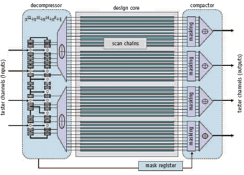
Figure 1. EDT compression technology embeds transform logic between few tester channels and many internal scan chains
During standard scan ATPG, only a small percentage of scan cells can be loaded for each pattern to detect targeted faults and most scan cell values are loaded with random data. EDT is more efficient because the compressed stimulus from the tester is transformed and expanded into many internal bits within the same cycle. Thus, a few tester channels can load many internal chains in parallel. Then, the output compactor combines many internal scan chain responses into a few tester channels. If an unknown state (often called an ‘X value’) is found to interfere with a targeted fault, it is masked and prevented from interfering with test coverage. EDT technology enables the highest possible scan test coverage, helping to overcome manufacturing challenges.
When fewer device I/Os are available
There is a growing demand to re-allocate pins for specialized functions other than test. Designers are embedding many more functions on a device such as specialized I/O. As a result, SERDES and other I/Os have been allocated to many of the available device pins with the result that test I/O capacity is being squeezed down. However this can help to control costs. In some cases, the application itself dictates that few I/O pins are available for test. Smart cards, for example, often have as few as five pins on the package.
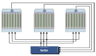
Figure 2. Multi-site test addresses several devices in parallel
Another motivation for the use of fewer test pins is to reduce the cost of the device I/O and the tester, and also to cut the tester interface’s cost and complexity [2]. An extreme case is multi-site test where many devices are tested in parallel [3] (Figure 2). Every test pin used is multiplied by the number of multi-site devices. In such a scenario, using only a few test pins is very beneficial. As the test interface increases, so do the cost and the chance of a bad test contact.
High quality test with fewer pins
The test environment is being pushed in two directions: more tests are required to maintain quality as device complexity increases and fabrication-process defects change, yet fewer pins are available to support changes in device pin allocation.
Traditional scan testing uses connections from the tester to the scan chains and to every functional I/O pin to force data and to capture responses at these pins. Today, the device I/O can have many hundreds of pins, a costly interface. As an alternative, an approach called reduced pin-count test (RPCT) provides control and observational access close to the I/O pins but without tester contact (Figure 3). The basic idea behind RPCT is to re-use boundary scan cells located at functional I/O pins for control and observation during scan testing.
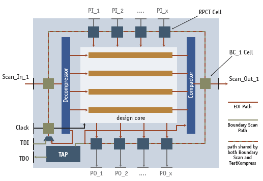
Figure 3. RPCT techniques indirectly control and observe functional IO through boundary scan cells so that tester contact is not necessary
These cells are controlled through the boundary scan state machine and a four- to five-pin test access port (TAP). The TAP is set up so that after initialization, each boundary scan cell behaves as if it were a normal scan cell. The TAP remains in a static state after being initialized. Thus, ATPG has access close to the functional I/O pins during normal scan test pattern generation. This means that connection to the functional pins is not necessary during scan test. Even at-speed scan testing can be performed efficiently by using RPCT techniques where the boundary scan cells stay in shift mode during the at-speed launch cycle to avoid launching X states from the unconnected functional I/O [4].
At some point, the functional I/O needs to be verified for correct operation and parametric performance. Testing with contact to functional I/O can be delayed until the packaged device is tested. As a tradeoff for tester and test-fixture savings, wafer test can accept a small amount of missing contact coverage at the functional I/O.
The RPCT method is available to reduce the functional I/O. What remains is to minimize the connections to the test port. Logic built-in self-test (LBIST) can be used here. At this point, LBIST technology provides effective testing but is based on random patterns and cannot reach the test quality requirements for some products without adding deterministic scan patterns.
Most test pins used during scan testing are for scan channel input and output ports. These pins can be reduced by using aggressive embedded compression with very few channels. This can result in either significant coverage loss or inefficiencies, but such problems can be avoided by applying automatic X-masking. In the past, masking often resulted in inefficient capturing, required a lot of mask data reduction, or masked most chains, also hurting compression. But recent masking technology, such as that used in EDT Xpress [5], provides more flexible automated masking modes from minimal mask data. As a result, very high compression is possible for one or two scan channels even with a high population of X states.
Effective test compression for one or two channels is being effectively used today. We recently reported effective test compression results from just one or two scan channels in which the test quality as compared to traditional scan was maintained [6]. One example showed that tester channels could be reduced by 16X from 32 channel pairs to two while still running test patterns 8X faster than the 32 for traditional non-compression baseline. Also, the ability to perform scan diagnostics was preserved so that the diagnostics resolution was similar to non-compression scan diagnostics results.
Conclusion
Production test is now moving not just to scan compression technologies but scan compression augmented with minimal test interfaces and RPCT techniques for functional I/O pins. These approaches are meeting the demands for high-quality test without increasing cost, while also allowing more pins to be used for specialized I/O. In addition, by using low pin-count test methods, modern production approaches such as multi-site test and volume diagnostics can be supported.
References
- J. Rajski et al., “Embedded Deterministic Test for Low Cost Manufacturing Test”, Proc. Int’l Test Conf. (ITC ‘02), IEEE Press, 2002, pp. 301-310.
- L. Boon, “Test Cost Saving and Challenges in the Implementation of x6 and x8 Parallel Testing on Freescale 16-bit HCS12 Micro-controller Product Family”, Proc. IEEE Workshop on Electronic Design, Test and Applications (DELTA’06), 2005.
- S. Goel, et al., “On-Chip Test Infrastructure Design for Optimal Multi-Site Testing of System Chips”, Proc. DATE 2005.
- J. Jahangiri, et al., “Achieving High Test Quality with Reduced Pin Count Testing”, ATS 2005.
- R. Press, “Embedded Compression for Production Test”, Evaluation Engineering, October 2007.
- 6. T. Kobayashi et al., “DFT Approaches Enable Mass Production Test”, Proc. Semicon Japan 2007, Dec. 2007.
Mentor Graphics
Corporate Office
8005 SW Boeckman Rd
Wilsonville
OR 97070
USA
T: +1 800 547 3000
W: www.mentor.com