Have your cake and eat it: the future of simulation and verification
T he explosion in consumer electronics, especially in the wireless/handheld devices marketplace, has placed a tremendous technical and business burden on engineers in the design of these products. Design teams carry the responsibility of catering to often conflicting and always challenging product specifications. The product needs to be optimized on multiple demand vectors with little or no maneuverability on the specifications and must hit a high-volume market within a very small time-window.
Digging down the design-chain, the picture does not get any prettier. The designs tend to be a confluence of multiple styles but with very familiar ingredients: ASIC blocks, custom digital logic, third-party and existing reusable intellectual property (IP), a handful of memories (ROM/RAM), and some analog blocks including the I/O pads. Each block must be simulated and verified for functionality and timing. It must then be stitched together with other blocks and re-verified and re-simulated. Since the simulation profiles of these building blocks vary widely both in complexity of simulation and the length of time taken to simulate, designers have to exercise great discretion in choosing the verification methodology and tool-set.
As demand for higher performance and smaller form factors grows, designers are compelled to consider migrating to smaller geometries. However, for every advantage these successive nanometer processes provide, they carry with them an equally significant set of design obstacles. One of the many emerging problems in nanometer design is the circuit simulation of sensitive subblocks and verification of the large blocks. This problem is rather unique in its scale and scope as the simulation needs of the circuit designers are on the opposite sides of the simulation spectrum. Circuit designers want to simulate their designs extremely accurately but they also want to verify them as rapidly and as comprehensively as possible. These two seemingly diametrically opposed constraints place significant demands on the simulator and the simulation resources.
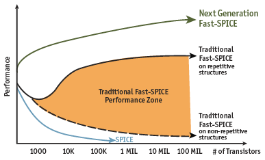
Figure 1. Performance trends of circuit simulators over large designs
Current circuit designs are complex in functionality and massive in implementation. Consider the profile of a potentially new design to be developed in 2007: 16 million transistors, at least 500 million RC parasitic components, an on-chip local clock of 450 MHz and over 30% of the content being analog/RF. To be used in an increasing number of untethered applications, this design must operate at 1V or less and consequently, needs to be highly power-efficient.
Shortened design cycles and ever-shrinking market windows would require about 25% of the design to be pre-existing IP, either from other designs/design groups or from thirdparty vendors.
To further add to this complexity, 60% of the designs will be implemented at 90nm or less. The current practice of estimating the transistor behavior on silicon is being done through esoteric models and is just that – an estimate.
Such estimates served well when digital operations were granular enough to ignore a lot of electrical (noise, leakage current, coupling, etc.) and physical effects (well proximity effect (WPE), sidewall capacitances, etc.). As geometries and voltages scale down, these effects can no longer be ignored and the ability to accurately predict silicon behavior has become much more complex.
In an attempt to account for these effects, transistor models at nanoscale have incorporated parameters designed to reflect physical effects such as WPE, STI (shallow trench isolation) LOD (length of diffusion) effects, sidewall and non-linear capacitances, resistances, and so on.While this intricate modeling helps to provide a better estimate of the behavior of the circuit in silicon, it has the unwelcome side effect of increasing the simulation time by as much as 20%.
The set of attributes that circuit designers involved in nanometer design simulation and verification care about can be distilled into three categories:
- Speed. How fast can I run the current circuit, sub-block or design?
- Capacity. How large a design can I simulate?
- Accuracy. How accurate do I need the results to be?
It is the application of these attributes to the simulation and verification of the overall circuit and each of the sub-blocks that determines the integrity of the design and quality of the product. Each sub-block, when simulated at the transistor-level, may present different simulation profiles in terms of accuracy and complexity. At this level, the simulator must provide the functional coverage needed to verify relatively large sub-blocks, while still delivering the accuracy needed to capture the ‘real’ effects at that level. However, simulating sub-blocks in isolation does not provide a complete picture of a chip’s behavior. It is essential to stitch these blocks together and simulate the resulting larger block, one that may consist of millions of devices and hundreds of millions of parasitics. Therefore, a simulator with larger capacity provides the benefits of higher accuracy and broader coverage, thus leaving less room for guesswork and error.
Finally, nanometer designs require better insight into a circuit’s behavior at the transistor level and the simulator needs to be able to accurately predict/estimate the behavior of the device on silicon. Needless to say, without accurate results, the rest of the simulation is an exercise in futility.
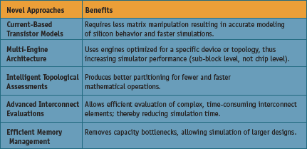
Figure 2. Novel approaches for next generation Fast-SPICE simulators
Tight resources
It is an indisputable fact that design teams are almost always short of simulation and verification resources. Even as CAD groups and design teams are moving from expensive servers to cheaper Linux boxes, they are unable to meet the simulation and verification requirements of emerging designs.
As disparate technologies continue to converge, greater numbers of features are crammed onto the same device with a corresponding increase in the functionality that must be tested. The verification time increases in a quadratic manner with increasing functionality.
For a typical chip design in 2005, an average of 24% of the time was spent in functional verification and an additional 28% is spent in physical design and verification – a whopping 52% of the design cycle. With the average number of machines per designer being close to three, the time spent in verification becomes so much more significant. It is no wonder that the productivity gap diverges as much as it does as design teams tackle larger and larger designs.
How, then, are circuit designers supposed to overcome these seemingly insurmountable verification and simulation hurdles?
The traditional simulation tools, while performing well at the sub-micron design level, rapidly degrade at the nanometer design level. This calls for radical approaches to resolve these impending issues. There are two potential ways of resolving the speed, capacity and accuracy issues:
- Use a very fast, high-capacity, transistor-level simulator that can accommodate a wide range of circuits and provide rapid results with high accuracy.
- Use a platform that optimally leverages new and existing hardware by enabling distributed, high-speed simulation. Here, we will focus on the first of these solutions.
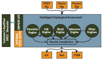
Figure 3. A sample multi-engine architecture for next generation Fast-SPICE simulation and verification
Accurate SPICE simulators derive their accuracy from translating a circuit into linear equations and solving these linear equations through matrix operations. As the size of circuit grows, its SPICE matrix tends to get very large and solving this matrix is computationally intensive, even prohibitive beyond a relatively small circuit size. This is one of the key reasons for these simulators’ high accuracy but low speed and low capacity. Traditional Fast-SPICE simulators have devised ingenious methods to identify replicated circuit structures and reduce the number of equivalent circuits by partitioning based on electrical dependence. This essentially reduces the size of the matrices and hence provides greater speed and capacity.
However, in creating these shortcuts using the same voltage-based models as accurate SPICE simulators, users of traditional fast-SPICE simulators are forced to trade off between the speed of simulation and the accuracy of results (Figure 1). This approach becomes cumbersome and inefficient for nanometer designs.
Novel thinking
Fortunately, in the past year, several novel approaches (Figure 2) have arisen in the industry to circumvent the shortcomings of traditional fast-SPICE while maintaining the desired characteristics of high-speed, large capacity and greater accuracy in simulations – akin to proverbially having your cake and eating it too. Some such approaches include:
- Current-based transistor models. Active MOS devices are intrinsically current-based devices and a current-based model reflects this behavior significantly better than a voltage-based model.While a voltage-based model provides some key information about transistor behavior, it has several drawbacks in terms of accuracy for current measurements, stability in simulations and the size of the resulting matrix. Current-based models are not only as accurate as SPICE or SPICE-like models but also simplify the topological structure of the equivalent circuits. This greatly improves the solution of non-linear equations and matrix solutions. Additionally, current-based models are very efficient in device representation and require less memory than voltage-based models.
- Multi-engine architectures. A circuit can be decomposed into basic transistors, logic cells, cell blocks, interconnect structures and multiple other design entities, that each share a unique simulation profile.When considering a circuit for simulation, traditional fast-SPICE simulators use one monolithic engine to tackle all the varied elements in the circuit. This is inefficient and the accuracy degrades as the processes get complex (as they do in nanometer designs). Having a multi-engine architecture (Figure 3) helps in a couple of ways:
- It uses a dedicated engine to optimally handle each particular circuit component.
- It provides an efficient infrastructure for managing and parallelizing the simulations.
The use of multiple dedicated engines also results in the ability to produce greater accuracy in the simulations while increasing the speed of simulations.
- Intelligent topological assessments. Recognizing an independent portion of a circuit, especially when there are millions of coupling caps and resistors, is tricky. Given that this dependence varies with input and resulting control signal changes, partitioning a circuit becomes all the more challenging. Algorithms that can intelligently recognize these partitions/topologies and appropriately guide the simulation to use these partitions are crucial to the speed and capacity of the fast-SPICE simulation.
- Advanced interconnect evaluations. For nanometer designs, parasitic loads are the predominant factor in gate delays. The composition of the interconnect between the driver and the driven is complex at best. Dedicated algorithms have been developed that recognize these interconnects and model them appropriately without affecting either the accuracy or the effects of that interconnect. This greatly enhances both the simulation time as well as the capacity of the fast-SPICE simulator.
- Efficient memory management: The memory requirements of full-chip simulations have already crossed the 4G limit available on most commercial machines. The increase in the number of transistors in today’s nanometer designs and the explosion of parasitic elements only exacerbates this capacity problem. The simulator, therefore, needs to efficiently store and manage the information needed for key partition simulations and then collate all the results in the final run. This memory efficiency helps the designer perform full-chip simulations and verify a greater set of functionality than was previously possible.
This article was intended to provide an alternative, albeit important, insight for design managers, CAD managers and technocrats into the impending challenges for simulation and verification of nanometer designs at the transistor level.
As 90nm and 65nm designs become mainstream, circuit and product designers will take on the thankless task of simulating and verifying larger designs within increasingly shorter design cycles. The next generation Fast-SPICE simulators will incorporate the above mentioned radical approaches to help ease the onus on the designers and increase the design productivity dramatically.