Embedded non-volatile configurable program storage
Processor program storage today
Most of the microcontrollers currently on the market store program code in one of three ways: in ROM on the same chip as the MCU; in embedded flash memory on the same chip as the MCU; or as external flash memory whose contents are downloaded to the MCU. Each of these non-volatile memory techniques has shortcomings that add cost, reduce data and firmware security, or limit device flexibility.
Embedded ROM
Embedding ROM on the same chip as the MCU provides low-cost storage, since the ROM is fabricated in the same logic process as the MCU-based chip and it does not add any significant area to the chip. However, with mask-programmable ROM, the MCU’s program code is configured and finalized during chip fabrication. The feature sets of consumer products can change very quickly, as often as every three months. Market demand may require a different version of a chip’s firmware for each different feature set.
In a typical chip-design project, firmware is directly in the project’s critical path. Every change in the contents of a masked ROM requires an NRE charge, which is a substantial burden for today’s most broadly used 130nm and 180nm processes and will increase again as 90nm becomes more commonplace. Furthermore, each change incurs an eight-to-12 week turnaround, sometimes even longer if the designer’s foundry is running at full capacity. Finally, there is additional cost associated with managing the inventory of chips that comprise derivative products or upgrades of a basic device.
Another problem with ROM storage of program code is that it is relatively easy to steal that code — code which represents significant intellectual property to the chip developer. Program code defines the value of the MCU, often through the definition of proprietary processing algorithms.
Embedded flash
Embedding flash memory on the same chip as the processor provides a way of reconfiguring firmware in the field. However, flash is expensive to implement, since even a few bits require extra masks and masking steps beyond those that a regular high-speed logic process uses. Wafer costs increase around 30-50% for adding embedded flash to a chip.
A second problem with flash is its scalability to new processing nodes. Migrating a chip to a newer silicon process that supports higher logic and memory density lets the chip vendor put more functions on the chip. This helps to satisfy consumer electronics’ demand for ever increasing feature sets, to increase chip performance, and to put a current chip’s functions on a smaller, cheaper chip.
Unfortunately, flash and other charge-storage types of floating-gate non-volatile memory (NVM) technologies are limited in their ability to store charge since, as transistor oxides get thinner, direct tunneling through the oxide occurs and the charge tunnels (drains) off. Flash charge-storage technologies have scaling limitations between 80 and 85 angstroms for the wafer’s tunnel oxide thickness – that is, the thickness of the tunnel oxide flash must have to reliably hold the charge once it is stored. Logic CMOS gate oxides are currently much thinner, in the range of 30 angstroms.
Moreover, the lower voltage that is needed to achieve tunneling, associated with chips fabricated at advanced process nodes, limits the spacing between storage cell elements — the transistors. In other words, with flash, there must be some defined amount of isolation between transistors that limits its implementation. Current flash technology lags one-to-two process generations behind leading-edge logic.
Finally, flash also has security limitations. Voltage contrast and other sophisticated scanning techniques can provide a means of reading information stored in flash memory, thus compromising the security of the program code if it is stored in that medium.
Separate flash chip

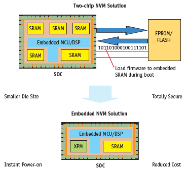
Figure 1. Example application for high bit-count embedded CMOS NVM
Storing firmware or other code in an external flash chip and downloading it to the processor chip leads to the configuration shown in the top portion of Figure 1. During system power-up, firmware is transferred to SRAM embedded on the processor chip and the system ‘boots up’.
Replacing the external flash chip, and SRAM with a non-charge-storage type of NVM can significantly reduce the size of the processor chip. In addition, the firmware is now secure – being permanently hidden within the chip, it is virtually impossible to steal. System cost is reduced by eliminating the cost of the external flash chip and by reducing the processor chip’s real estate occupied by the SRAM used to store downloaded code from the external flash chip. Additional advantages are that packaging, engineering, and inventory-overhead costs are reduced by using a single silicon platform. Furthermore, the system can now provide instant-on performance without a boot-up delay
Attributes of low-cost, secure NVM
To circumvent the problems associated with flash and ROM for program-code storage, Kilopass Technology has developed, and proposes as an alternative, XPM — a secure, one-time-programmable (OTP) NVM memory that is implemented in a standard high-speed logic process and is field-programmable. Unlike flash, XPM does not depend on the injection and tunneling of charge to and from a floating gate to store ones and zeros.
Instead, the XPM memory cell uses a very short channel MOS transistor that looks like a capacitor (an open circuit) in the unprogrammed state. XPM is similar to an anti-fuse technology in that it is a closed connection after programming, but unlike current anti-fuse technologies the XPM cell’s connection is located in the CMOS transistor’s gate-oxide, not between metal layers. Since the XPM cell comprises, basically, standard CMOS transistors, its technology will track to new CMOS logic-process nodes.
When programmed by a short voltage pulse, the gate oxide suffers a permanent breakdown and the transistor conducts like a resistor (a closed circuit). However, the memory cell does not add any additional leakage current during normal operation. The current needed to program an XPM memory block is low and a 1Mbit memory can be programmed in just a few seconds.
Reconfigurable NVM such as flash lets a system developer modify the system in the field to account for software upgrades or other modifications. However, reconfigurability with flash comes at a cost — larger memory cell size, additional processing cost, and/or a lack of scalability to
leading-edge CMOS processes. There are many instances in which a one-time programmable (OTP) NVM like XPM can be used where traditional reconfigurable flash NVM was originally deployed. The trick is to include one or more uncommitted sectors in the OTP memory along with the sectors storing existing program code. To upgrade one of the program-code modules, the upgraded module is programmed into an unused memory sector and control logic is switched to point to the updated module. Thus the memory, which is OTP on a cell-by-cell basis, is actually ‘few times programmable’ at the system level.
Program storage application example
Flash media controller
A good example of the use of embedded, field-configurable NVM is in the FS7821 flash media controller from the Fulhua Microelectronics Corporation (known as FameG). As a fabless SoC ODM operating in Shanghai, HsinChu and Taiwan, FameG works with manufacturing and intellectual property (IP) partners. The company also intends to work with other semiconductor product companies to assist them in re-targeting their chips for local manufacturing and to re-engineer their application solutions to meet the growing needs of the Greater China region.
FameG develops and acquires IP, and develops platform-based SoC chips, development support tools, and embedded software that their customers and partners can use to develop their own chip products and application solutions.
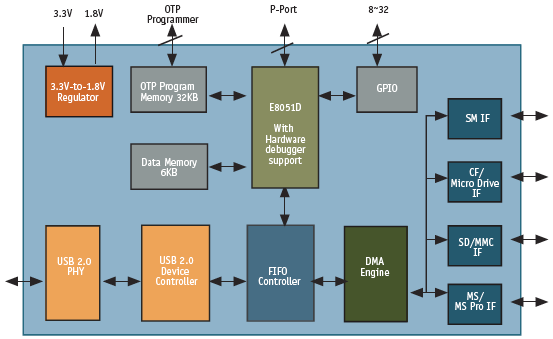
FameG’s integrated standalone media controller uses an embedded E8051D microcontroller core to handle both data flow and control (Figure 2). In addition to the MCU, the FS7821 comprises a USB 2.0 high-speed/full-speed device controller, a USB 2.0 PHY, a DMA engine, an OTP non-volatile memory for program storage, a voltage regulator, and a FIFO controller. The controller interfaces to several storage media types, including SmartMedia (SM), CompactFlash (Card Type I/II), IBM MicroDrive, Secure Digital (SD), MultiMedia Card (MMC 4.0), Memory Stick (MS, MS-Duo), and Memory Stick-Pro (MS-Pro, MS-Pro Duo).

Figure 2. Block diagram of the FS7821 media controller
The USB 2.0 controller and PHY handle data transfers between the USB bus and the FS7821’s internal FIFOs at rates up to 480Mbps for high-speed and 12 Mbps for full-speed. Using an enhanced power-control circuit, the FS7821 complies with the USB specification for a low-power device.
The embedded E8051D high-performance 8-bit microcontroller is fully compliant with the industry-standard 8051. With a 1-T instruction cycle equal to the CPU clock cycle, the MCU has 10X the speed of the traditional 8051. Thanks to a built-in hardware debugger, the embedded software designer can easily develop and verify software codes via a familiar integrated environment such as Keil uVision. The E8051D core supports the command sets of the USB Mass Storage Class Bulk-Only Specification (Rev. 1.0), providing plug-and-play capability with the Windows operating system with no additional drivers. During operation, the MCU arbitrates data transactions between the USB host and various flash media, with the hard-wired DMA engine and optimized firmware providing greatly improved performance.
In this configuration, 32Kbyte of embedded Kilopass XPM OTP non-volatile memory store the E8051D’s program, reducing the need for — and cost associated with — external memory for program storage. Since firmware code can be externally downloaded to the OTP memory through a programming interface, it is easy to upgrade products that use the FS7821 media controller, such as adding MP3 decoding capability.


