Design of SoG with p-SI TFTs using AMS simulation for AMOLEDs
The use of poly-Si TFTs for active matrix OLEDs (AMOLEDs) allows peripheral circuits to be integrated on a glass substrate at low cost and reduces the number of external driver ICs. The prospect of such integration means it is likely that emerging system-on-glass (SOG) design projects will feature both analog and digital blocks, such as digital-to-analog converters (DACs), DC-DC converters, frame-memory, and timing controllers (TCONs). However, for all their benefits, SOGs today pose enormous challenges.
SOG is currently focused on analog design strategies and, consequently, transistor-level simulation techniques. These are slow, labor-intensive and have limited capacity. And in turn, the restrictions involved currently lead engineers to simulate circuits only partially, increasing the risk of re-spins. A good reason for this analog focus has been put forward. It is argued that poly-Si TFTs are not yet stable enough for standardization, and analog simulation makes the best use of their characteristics.
However, this paper proposes a new approach to this type of mixed-signal circuit design, using the example of a display driver integrated on glass. We believe that this technique, analog/mixed signal (AMS) simulation, offers major advances in capacity and speed over existing techniques, and will allow for the analysis of the whole signal, from peripheral circuits to the OLEDs.
The experiment
We conducted our experiment based on the simulation of the data and scan drivers for a 2” QVGA (320X240) display integrated on glass to compare the AMS simulation strategy against traditional SPICE simulation.
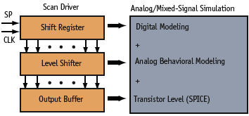
Figure 1. Block diagram of a scan driver and its simulation methods
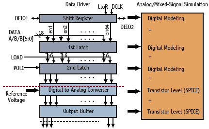
Figure 2. Block diagram of a data driver and its simulation methods
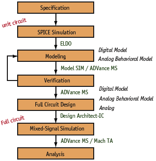
Figure 3. The AMS simulation flow showing EDA tools used
For the scan driver, it normally takes too long time to simulate its whole 240-stage output with SPICE. Typically 20 stages are simulated during verification.Meanwhile, the data driver has 360 DAC outputs but only one DAC output can normally be simulated by SPICE because of time and capacity limitations.However, the full outputs of both were used here for a realistic SPICE vs AMS comparison. For the scan driver, the shift register, the level shifter, and the output buffer blocks were simulated as a digital block using VHDL, the analog behavioral model block was simulated using VHDL-AMS and the analog block using SPICE (Figure 1). For the data driver, the digital blocks for the shift register, the 1st latch for sampling, and the 2nd latch for holding were modeled in VHDL. SPICE was used for the DAC and the output buffer to ensure the accuracy of the data driver (Figure 2).
Figure 3 shows the AMS simulation flow and the EDA tools that were used. First, unit circuits undergo SPICE simulation according to the specification. Based on the results, appropriate digital and analog behavioral modeling takes place (the range of this modeling depends on how much simulation accuracy is needed: e.g., the DAC circuit does not generally undergo analog behavioral modeling because of its effects on accuracy). As the modeling verification is completed using the SPICE simulation results, the full circuit – the analog block, the digital modeling block, and the analog behavioral modeling block – is designed for the full circuits simulation. Finally, the engineer analyzes the results of the circuits simulated by the AMS flow.
SPICE simulation
Scan driver
As noted, the scan driver has three main circuit blocks. The first, the shift register block, functions as a scan pattern generation and includes a shift register and a 3-input NAND circuit. The second, the level shifter block, converts low-voltage signals into high-voltage data. The third block, the output buffer, drives relatively large capacitance and resistive load.We used the ELDO program for SPICE simulation and the Level 62 RPI poly-Si TFT model. It took 61,486 seconds to run the 240-stage QVGA simulation. The total transient time, a two-frame period, was 0.034 seconds. There were 69,657 nodes and 10,611 components.
Data driver
The data driver has five main circuit blocks. The shift register makes the sampling clock for the 1st latch. The 1st latch, called a sampling latch, samples data by sampling the clock. The 2nd latch holds data sampled by the 1st latch until the load signal is triggered. The DAC converts 6bit digital signals to analog according to the reference voltage. Finally, the buffer drives and ensures exact gamma voltage control for the panel. A 1:2 DEMUX circuit (often used in low temperature poly silicon panels, so that only 180 DACs are required for QVGA resolution), and electrostatic discharge prevention circuits are also included in the data driver simulation. There were 162,038 components in the full data driver circuit for SPICE simulation. This simulation failed because the number of components exceeded computer memory and SPICE capacity, highlighting SPICE’s limitations.
Figure 4. Registered symbol of the shift register block for the scan driver in Design Architect-IC
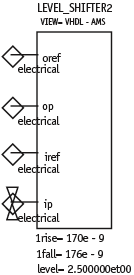
Figure 5. Registered symbol of the level shifter block in Design Architect-IC
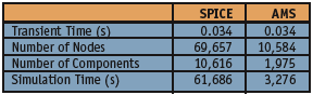
Figure 6. Comparison of simulation methods between ADVance MS and ELDO
AMS simulation
Scan driver
The shift register, a 3-input NAND, a 2-input NOR, and inverter circuits were modeled as digital circuit blocks by using VHDL with the ModelSim tool used for functional verification. The VHDL code was then compiled. Figure 4 shows the symbol in Design Architect-IC. Its input signals such as SDCLK, SDCLKB, SDOE, and SDSP are analog, which should be converted into digital signals for simulation through an analog-to-digital converter (ADC). The output is made up of NAND[i], NANDB[i], NOR[i], and NORB[i], analog signals converted from digital information through a DAC.
The level shifter circuit block is substituted with an analog behavioral model using VHDL-AMS. Figure 5 (p26) shows the registered symbol of the level shifter block. The modeling uses a simple ramp type of the pulse in which the rising time and the falling time are respectively 170ns and 176ns in the threshold of 2.5V (there is a maximum error value of 110ns when the pulse falls. Precision modeling can remove this error, but that is beyond the scope of this paper).
Thus, the digital and analog behavioral models were substituted for respectively the shift register and the level shifter block, though there was no change to the output buffer. Then, the scan driver was run through AMS simulation using ADVance MS. This took 3,276 seconds, approximately 19 times faster than SPICE. The number of components was 1,975, 18% of those used for SPICE. The results are summarized in Figure 6.
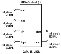
Figure 7. Registered symbol of the shift register block for the data driver in Design Architect-IC
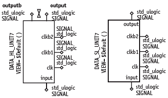
Figure 8. Registered symbol of the latch in Design Architect-IC
Data driver
The digital blocks in the data driver such as the shift register (Figure 7) and the latches (Figure 8) were substituted by digital models in Design Architect-IC. Inverters, and 3-input NANDs included in the DAC block were also modeled as digital blocks. Functional verification was then performed with ModelSim.
As a result, the components of the data driver were reduced to approximately 25%, from 162,038 to 40,393. The full data driver simulation was undertaken using ADVance MS in 21,504 seconds, whereas SPICE failed outright.
Conclusion
As technology advances, SOGs are likely to incorporate more and more both analog and digital circuits. Already an SOG circuit for a QVGA one-chip mobile driver IC without GRAM contains more than 200,000 transistors. SPICE’s capacity is not only limited to approximately 100,000 transistors, but it also takes a long time to run a simulation. The use of methodologies such as AMS simulation is therefore inevitable for SOG design and analysis.
For the next phase of our development of AMS simulation, we need to model the OLED pixel, pixel driving circuits, and the RC delay to achieve full panel simulation from peripheral circuits to pixel.We can then see the full panel’s characteristics before manufacture, and dramatically reduce design lead time.
Samsung SDI
428-5, Gongsae-dong
Kiheung-gu
Yongin-si
Gyunggi-do
449-577
Korea
www.samsung.com