Common pitfalls in PCI Express design
PCI Express is a point-to-point communications interface. It is neither an evolved nor enhanced form of PCI or PCI-X, but, essentially, a high speed, low voltage, differential serial pathway for communication between two devices, although it uses the same programming model as its predecessors. It employs a protocol that allows devices to communicate simultaneously by implementing dual uni-directional paths between them. This protocol is layered – it has a transaction layer, data link layer, and physical layer – and this article highlights a number of error-prone areas on each of those layers based upon our experience of verifying such projects.
An experienced PCI designer has a knowledge of configuration space, configuration cycles, memory cycles, device number, bus number, base addresses, TAG, and split cycles. Most are also comfortable with transaction layer concepts and terminology. But in general terms, it is the newer concepts which need special attention and are more error-prone. Let us now consider the problems on each layer in turn.
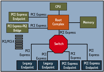
Figure 1. PCI Express topology
Transaction layer
The transaction layer is the upper layer of the architecture. It primarily assembles and disassembles the transaction layer packets (TLPs) used to communicate transactions (i.e., read, write). It also manages the credit-based flow control for TLPs.
Every request packet requiring a response is implemented as a split transaction. The packet format supports different forms of addressing, depending on the transaction type. The transaction layer supports four address spaces: the three PCI address spaces (memory, I/O, and configuration) and the message space.
Misinterpretation of the RCB parameter
A memory read request can be completed with one or multiple completions, based on the request size and the Max_Payload_Size. The read completion boundary (RCB) parameter determines the naturally aligned address boundaries in which a read request may be serviced with multiple completions. At times, endpoint designs assume that they can send 64byte-aligned completions when the RCB bit is set to 0. As a consequence, completions are incorrectly sent out broken into chunks aligned to the 64byte boundary instead of the 128byte boundary. The receiver treats these as malformed.
Max_Read_Request_Size register
PCI Express defines a capability structure in a PCI 3.0 compatible configuration space (first 256 bytes) for the identification of a PCI Express device, and it indicates support for new PCI Express features.
The device control register controls PCI Express device-specific parameters and has the field Max_Read_Request_Size. According to the specification, for memory read requests, the length must not exceed the value specified by this register.When Max_Read_Request_Size is misinterpreted, its value is used in the receive logic, and the size of the received read request is incorrectly compared with this register. As a consequence, a well-formed read request gets treated as malformed.
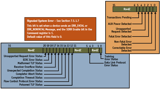
Figure 2. Error reporting registers
Implementing advanced error reporting
PCI Express defines two error reporting capablilites: baseline and advanced error reporting (AER). Baseline error reporting is required of all PCI Express devices and defines the minimum requirements. AER is for more robust error reporting and is implemented with a specific PCI Express capability structure. All PCI Express devices support existing, non-PCI Express-aware software for error handling by mapping PCI Express errors to existing PCI reporting mechanisms, in addition to the PCI Express-specific mechanisms. We have noted that when AER is implemented, the bits in the AER registers are updated correctly, but certain registers are omitted (e.g., status registers) that need updating in the standard PCI configuration space (Figure 2).
Data Link Layer
The data link (DL) layer serves as an intermediate stage between the transaction and physical layers. Its responsibilities include link management and data integrity, including error detection and error correction.
The transmission side of the DL layer accepts packets assembled by the transaction layer, then appends the cyclic redundancy check (CRC) and sequence number before submitting them to the physical layer for transmission across the link. The receiving DL layer is responsible for checking the integrity of incoming TLPs and submitting them to the transaction layer for further processing. On the detection of an error, this receiving DL layer requests retransmission of TLPs until information is correctly received or the link is considered ‘failed’.
PCI Express utilizes credit-based flow control. A receiving device advertises an initial amount of credit for each of the receive buffers in its transaction layer. A sending device counts the number of these credits that have been consumed. The sending device will only transmit a TLP when it does not exceed the credit limit.When the receiving device has processed the TLP, it signals a return of credits to the sending device, which then determines whether the next TLP can be sent based on the restored limit.
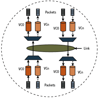
Figure 3. Virtual channel concept
Flow control
The combination of a virtual channel (VC) mechanism and traffic class (TC) identification is provided to enable differentiated services and quality of service (QoS) support for certain classes of applications. The flow control (FC) involved here was another key area where problems were observed. Device-under-test (DUT) behavior would be correct for VC0 (see Figure 3) possibly because this is initialized by default. Still, designers took good care of the credit flow information for VC0. But issues arose for VCx-credit handling. Specifically, updated FCs were not sent for VCx properly, leading to starvation. Another recurrent problem was that credit information was not updated for message packets. Certain message packets that were not supported by the DUT (e.g., system SSPL, vendor-defined) were simply ignored. They were not even considered when sending updated FC information, resulting in credits not being freed up and, again, starvation.
DL_Inactive status
The DL layer tracks the state of the link, communicates its status to the transaction and physical layers, and performs link management through the physical layer. The DL layer contains the data link control and management state machine (DLCMSM) that perform these tasks. DL_Inactive is the initial state following a PCI Express hot, warm, or cold reset.
With physical layer reporting, when the link is non-operational or nothing is connected to the port, the data link layer enters the DL_Inactive state. Upon entry to DL_Inactive, all DL layer state information should be reset to default values, and the contents of the DL layer retry buffer discarded. However, in some designs, the DL layer was not reset. Elements such as NEXT_TRANSMIT_SEQ, ACKD_SEQ, REPLAY_NUM and NEXT_RCV_SEQ were not set to default values. The retry buffer was not freed up on re-establishing the link. Also, the transaction layer (TL) packets received from the application layer were remembered and sent out even when the layer was in a DL_Down state (FC_INIT1). Therefore, the first packet was not sent with the sequence number as 0, the contents of the retry buffer were transmitted, and the credit logic became out of sync.
Replay mechanism
A receiving DL layer checks the integrity of received TLPs and submits them to the transaction layer for further processing. On the detection of any TLP error, the DL layer requests retransmission until information is correctly received or the link is judged failed. A replay can be initiated by the expiration of REPLAY_TIMER or by the receipt of a NAK.
However, during replay, we noted that some designs do not block the acceptance of new packets from the transaction layer, and therefore these packets appear in the middle of the replay. Other designs did not handle ACK/NAK during the course of replay and sent acknowledged packets again, degrading performance.
Lane count less than maximum supported
Assuming the maximum supported lane count to be eight but the link is established at four, various timers will remain at the eight lane configuration, specifically the AckNak_LATENCY_TIMER and the REPLAY_TIMER.
Physical Layer
The physical layer isolates the transaction and DL layers from the signaling technology. It is divided into logical and electrical functional sub-blocks and also includes logical functions related to interface initialization and maintenance. The physical layer exchanges information with the DL layer in an implementation-specific format.
Link training and status state machine
The physical layer converts information from the DL layer into an appropriate, serialized format and transmits it across the PCI Express link at a frequency and width compatible with the connected device. The link training and status state machine (LTSSM) is therefore one of its most important components.
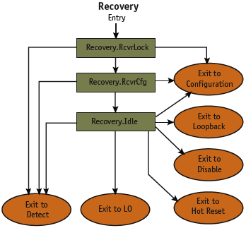
Figure 4. Recovery sub-state machine
Many designs had one error or another related to LTSSM state transitions. At times, designers ignored the transition control bits (hot reset, loopback, disable link, and disable scrambling) that are received as part of the training sequence ordered set. This leads to the DUT making incorrect transitions to L0 instead of desired states (Figure 4), and to LTSSM deadlock and unnecessary time-outs.
ASPM L0s entry
Tx_L0s and Rx_L0s are not kept independent. As a result the transmitter is forced to go to L0s when the receiver is in L0s. This blocks the packet’s transmission.
ASPM L0s exit
The transmitter sends out the N_FTS (number of FTS ordered sets) equal to the number it advertised and not based on the number it received. Thus, the device does not get the required time for transition to L0 from L0s. It might go to recovery after the N_FTS timeout.
Conclusion
Based on experience with the error-prone aspects of PCI Express design detailed above, we believe that compliance checklists must be a key component of the verification effort. Design groups should also make use of proven verification IP (VIP) that includes the following features:
- Support for all verification environments and languages, including SystemVerilog and SystemC
- An extensive number of assertions to check design behavior
- A compliance test suite based on the PCI-SIG checklist • Extensive error injection and detection capabilities
- An ability to create any real life test scenario
Designers and verification engineers also need to leverage advanced verification methodologies and should review error-prone areas more thoroughly. Using the back-to-back operation of proven verification IP will improve understanding.
Make compliance test suites a key component of the verification effort.When all is said and done, “To err is human.” The bugs are going to be there and, as noted from the examples above, designers do stumble upon common errors. Focus your efforts on defect prevention and the remedies that enable it.
nSys
35463 Dumbarton Court
Newark CA
94560
USA
P: 1-888-679-7462
F: 1-888-679-7462
W:www.nsysinc.com
Hi,
This is wonderful information. The data that you have shared will go a long way in designing good systems in which max utilization of the pcie bandwidth can be achieved.
I was checking on the internet but could not find any real information regarding heuristics and counters for correctable errors and uncorrectable errors. Do you have some data regarding how many un/correctable errors can you hit on a single pcie link? Can we write some heuristics algorithm which will monitor all the errors reported by the root complex and then heuristically determine that a particular link is bad (may be SN ratio is very bad? Any such numbers can help ppl in writing some driver which will do active monitoring.
Thanks