Characterizing process variation in nanometer CMOS
The correlation of a statistical analysis tool to hardware depends on the accuracy of underlying variation models. The models should represent actual process behavior as measured in silicon. This paper presents an overview of test structures for characterizing statistical variation of process parameters. It discusses the test structure design and characterization strategy for calibrating random and layout-dependent systematic components of process variation. It also shows measurement results from several fabricated structures in 65nm CMOS technologies.
Despite advances in resolution enhancement techniques (RETs), lithographic variation is still a challenge for sub-90nm technologies. Meanwhile, aggressive scaling has resulted in many non-lithographic sources of variation such as dopant variation, well-proximity effects, layout-dependent stress variation in strained silicon technologies, and rapid thermal anneal (RTA) temperature-induced variation. These sources must be characterized and modeled for improved model-to-hardware correlation.
Process monitoring has traditionally relied on measurements taken from a small set of test structures placed in the scribe line. These structures are inadequate in characterizing different sources of variation and can show a large offset from the device behavior on the die. Hence, it is increasingly important to develop characterization test structures that provide insight into the magnitude, nature (systematic vs. random), and scale (local, across-die, across-reticle, across-wafer, wafer-to-wafer, and lot-to-lot) of different sources of variation.
This paper considers test structures required for characterizing random- and layout-dependent systematic components of process variation. For random variation, we discuss the design of a device characterization array fabricated in a 65nm silicon-on-insulator (SOI) process. The I-V measurements from the device array are used to extract intrinsic random fluctuations in device parameters. The FET array structure, though very useful, requires several hours of tester time in an offline environment. This highlights the importance of easily testable structures and the paper presents a test method for rapid in-line characterization for random threshold voltage scatter. The paper also discusses the importance of the layout-dependent systematic component of process variation. This component is predictable and can be modeled as a function of layout parameters. We consider sources of layout-dependent variability and present test results to demonstrate the impact of layout on device performance in recent technologies.
Characterizing random variation
Local random variations can cause mismatch in two identical devices placed next to each other. Such variations are unpredictable and are caused by random uncertainties in the fabrication process such as microscopic fluctuations in the number and location of dopant atoms in the channel region and polysilicon gate line-edge roughness. Random local variations are critical for circuits that rely on relative device matching (e.g., SRAM cells). Characterizing random mismatches requires test structures with closely placed devices where each device can be measured individually. Variations should be measured at the individual FET-level because test structures such as ring oscillators mask random variation due to averaging across many devices. Furthermore, a large number of devices should be measured for statistical confidence.
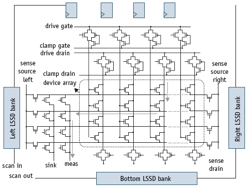
Figure 1. Device array for characterizing random variation
We designed an addressable array-based test structure for statistical characterization of random parameter fluctuations in MOSFET devices in a 65nm SOI process. The test structure features a large array of densely populated small devices. The electrical characteristics of each device can be measured independently. Figure 1 shows the schematic of the test structure. It contains a 1,250umX110um array with a total of 96,000 devices placed in 1,000 columns (96 devices in each column). The fundamental operation of the array is very simple – the device-under-test (DUT) is activated by selecting the corresponding row and column. Once selected, gate and drain voltages are applied and the device current is measured. Several concerns must be addressed to ensure reliable measurement. The most important include:
- The measurement and compensation of IR drop in the row and column switches and routing wires.
- The measurement and mitigation of leakage of nonselected devices.
For IR drop, a four-point sense-force configuration is used. The drain lines are typically forced from the top and sensed at the bottom.
Similarly, sense capability is added to measure the row voltages at both ends of the array. As shown in Figure 2, the setup steers all current to the left, hence the sense voltage at the right end is used as a measure of the exact voltage appearing at the source node of the DUT. The difference between the sense voltages at two ends of a row can also be used as an indicator of the IR drop due to parasitic resistances.
To minimize leakage of non-selected devices, clamp capability is added. During measurement, the gate and drain terminals of the non-selected columns are clamped to their respective clamp voltages. The gate-clamp voltage can be chosen to drive the gate-lines of the non-selected columns with a negative voltage to minimize their leakage currents.
The current steering logic directs the current of the DUT row to the measuring pin and the currents of the remaining rows to the sink pin. Current steering is useful in measuring leakage currents when the DUT is biased at a small gate voltage. However, while measuring on-currents, the sink devices must be cut off to prevent a large voltage drop in the column drivers.
The current steering devices are made of thick oxide to reduce their gate leakage current. Level-sensitive scan design (LSSD) latch banks are placed at all four sides of the array. The top and bottom banks are used to select the column under test for forcing and sensing gate and drain voltages, as well as to place non-selected columns at the clamp voltage. The left and right banks set up proper measure, sink and row-sense selection switches for each row.
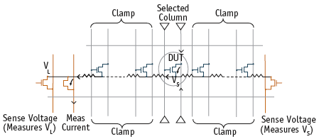
Figure 2. Sensing mechanism for handling IR drop
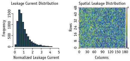
Figure 3. Measure leakage histogram and spatial leakage distribution
The manufactured dies were packaged and I-V characteristics of several devices measured. The uniform layout of the array provides an ideal topological environment for intrinsic random variation measurements. Figure 3 shows the sub-threshold leakage histogram and spatial distribution of the leakage as obtained from the measurement of 8,000 devices in the array. As expected, the sub-threshold leakage shows a lognormal distribution. Negligible spatial correlation is observed indicating a strong random component. Random threshold voltage (VT) scatter can be extracted from the electrical behavior of the measured devices.
Test time is a challenge with the FET array-based structures required for random variation characterization. The VT characterization process is quite slow because the VT of each device must be measured and extracted individually.
However, we can speed up the VT scatter characterization by exploiting the fact that the drain current (IDS) of a device is a function of voltage overdrive and not of gate-tosource voltage (VGS) and (VT) separately. Therefore, if we can force the same current IDS and drain-to-source voltage (VDS) through different devices, each device should have the same overdrive (VGS – VT) irrespective of the absolute VT value. Consequently, if dopant fluctuation causes the VT of a device to shift by a certain value then its VGS will shift by the same value to keep the overdrive constant. Hence, VT variation can be measured by monitoring the variation in VGS.
Figure 4 (p.36) demonstrates a circuit implementation of this concept where a constant current is forced through a DUT. A unity gain source-follower stage senses the source voltage and adjusts the drain voltage to fix VDS across the DUT. This forces a fixed IDS and VDS through the DUT. VDS across the DUT can be controlled by changing the bias current Ip of the source-follower. If VT of the DUT changes, it causes the source voltage of the DUT to change by an equal and opposite value. The VT scatter characterization process steps through each device in the array and measures the threshold voltage shift of the device by sensing the corresponding source voltage through the sense source line. The standard deviation of VGS around its mean value represents the standard deviation of VT. The reference value of VT can be measured by fully characterizing and extracting VT for any one arbitrary device in the array. The mean (nominal) value of the threshold voltage is obtained from the extracted VT of the fully characterized device and its measured VGS offset value. For example, if the threshold voltage of the device is 300mV and its measured VGS offset with respect to the mean VGS value is +50mV, it indicates then the nominal VT of the process is 250mV.
Figure 5 shows the experimental VT distribution obtained by measuring VGS fluctuations of 8,000 devices in the array. Significant speed-up is obtained because we take only one voltage measurement at each device before stepping to the next one. We also measured the electrical characteristics of a few sample devices in the array to characterize the impact of VT fluctuation on device performance. We selected two devices in the array that showed VT (or VGS) shifts of +3? and -3? respectively and compared their characteristics to a device with nominal VT. Figure 5 shows the comparison results. The VT offsets extracted from these characteristics agree well with the VT offsets measured using the source voltage monitoring scheme.
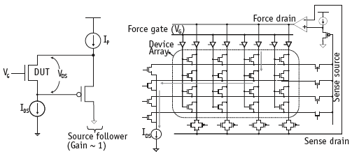
Figure 4. Circuit configuration for measuring V Toffset of a device- under-test (DUT) and corresponding array
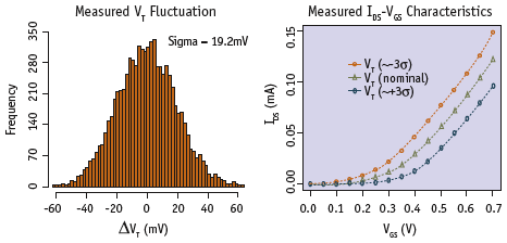
Figure 5. 5 Measured histogram of threshold voltage fluctuation and I DS-VGScurves for the three devices in the array with their threshold voltages at -3?, nominal and +3?point
Characterizing systematic variation
We can classify systematic variations as across-field (position in reticle) and layout-dependent variations. Across-field systematic variations are caused by photolithographic and etching sources such as dose, focus, and exposure variations, lens aberrations, mask errors, and variations in etch loading. They exhibit strong spatial correlation and can be characterized by embedding test structures at several positions in the reticle. Across-field variations can cause identical devices at different locations to behave differently. Layout-dependent variations, on the other hand, can cause two different layouts of the same device to have different characteristics even when the two instances are located close to each other. Layout-dependent variations are different from random ones because they are predictable and can be modeled as a function of deterministic factors such as layout structure and the surrounding topology.

Figure 6. Measured dependence of mean ring oscillator frequency on polysilicon contact landing pad to the diffusion region spacing
Several factors can cause a device’s behavior to depend on its layout. For example, variation in poly pitch and orientation can affect the critical dimension (CD) variation. Restrictive design rules (RDRs) and optical proximity correction (OPC) can minimize variation, however many layout configurations can still cause a systematic shift in the device parameters. For example, the spacing of the polysilicon contact landing pad to diffusion (active) can impact performance through corner rounding or poly flare. Figure 6 indicates a layout-dependent shift in the mean ring oscillator frequency as measured in 65nm SOI. Similarly, different configurations of the active area and contacts can also induce deterministic variations in device characteristics.
Other sources of variation can cause a device parameter to vary with its local layout environment. The well-proximity effect is a well-known example of local layout-dependent VT variation, caused by the scattering of dopant ions from the edge of the well-masking photoresist layer during deep well implants in bulk technologies. The scattering increases the surface implant dose in devices located near the edge of the well, resulting in a layout-dependent VT offset.
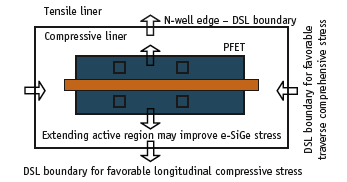
Figure 7. Layout dependence of dual stress liner (DSL) and embedded SiGe source/drain technology
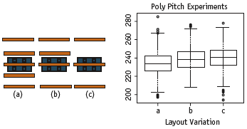
Figure 8. Measured on-current for three different layout configurations in a 65nm bulk technology
Stress is another source of layout-dependent variation. Several techniques have been developed to introduce uniaxial stress in channel areas for carrier mobility enhancement. These include the dual stress liner (DSL). The effective local stress seen by a device depends on the position of the DSL boundary (Figure 7). The effectiveness of the DSL also depends on layout parameters that interrupt liner films such as contacts. Other strain engineering techniques show layout dependence, including embedded SiGe (e-SiGe) source/drain technology for PFET mobility enhancement. As shown in Figure 7, the amount of e-SiGe stress depends on the active region around the device.
Furthermore, shallow trench isolation (STI) introduces an unintentional compressive mechanical stress that can cause device performance to vary with the density of the STI region around the device. These sources of layout-dependent stress variation are deterministic and must be characterized and modeled.
Unlike random variation, the layout-dependent effects can be characterized by ring oscillator-based structures. Ring oscillators have many advantages over FET array-based structures in characterizing systematic variations. Rings average the random variation across oscillator stages and hence can be used to measure systematic shifts in device characteristics without a large set of measurements. More importantly, ring frequency can be measured easily using frequency counters.
Ring oscillators also include AC effects and are more representative of device application in a real circuit. First-order capacitance information can be obtained from the rings by measuring the average current drawn during their operation. For a ring with n stages and oscillation frequency, F, the capacitance per stage, C, can be expressed in terms of average transient (IDDA) and quiescent currents (IDDQ):
However, rings are not suitable for studying all layout-dependent variations. A ring oscillator provides a single frequency data point that may include the cumulative effect of multiple sources of variation. For example, a layout variation (say, DSL boundary) may increase the NFET drive strength and slow down the PFET device simultaneously resulting in no discernible variation in ring frequency. If the effect under study is well understood, smart rings can be designed to accentuate the effect. However, more often than not, the sources of variation and their interactions are not clear.
Hence it is useful to supplement the ring oscillator structures with complementary FET arrays that can be measured if additional information is needed. However, the number of experiments required to cover the entire layout space is large and tester time may significantly limit the detailed FET measurement option. We have fabricated several ring oscillator and device array-based structures to study and characterize layout-dependent variations.
Figure 8 shows an example of a layout experiment and corresponding measurement results from a device array designed in 65nm bulk CMOS. The experiment was designed to characterize the impact of neighboring poly configurations on device performance. For each layout style, we measured on-currents of a large number of devices. The data is shown in Figure 8, right. The measurements show a clear layout-based systematic variation in the on-currents.
There are other sources of variation that depend on layout density in a larger window. One well-known example is pattern-dependent dishing and oxide erosion during copper chemical mechanical polishing (CMP). RTA may also induce layout density-dependent intra-die variations. During RTA, local anneal temperature can vary across the die due to differences in the radiation reflectivity of the layout patterns. The die regions with higher local anneal temperature result in better thermal absorption of junctions resulting in lower VT and lower extrinsic resistance of the devices. Characterizing these variations presents an additional challenge because of the difficulty in isolating the predictable layout-dependent part from the unpredictable across-field systematic variations.
Conclusion
Process variation can be caused by many sources with each exhibiting a different dependence on layout and design parameters. One must identify, characterize, and model all sources of variation for better model-to-hardware correlation. In spite of significant research into modeling process variation, however, several challenges remain in closing the gap between our modeling capabilities and actual silicon reality.
Acknowledgements
We would like to thank our colleagues Frank Liu, Dhruva Acharyya, Jerry Hayes, Anne Gattiker, Chandler McDowell from the IBM Austin Research Lab, and Jim Plusquellic from the University of Maryland, Baltimore County for their contributions to design and testing of the test structures discussed in this paper.
IBM Austin Research Laboratory
11501 Burnet Road
Austin
TX 78758
USA
T: +1 512 838 8072
W: www.research.ibm.com/arl/
But looks like this structure will take lot of Si area, which will be a big concern. I am not sure if this structure is worth adding on Si.