Automating design for high volume consumer markets
There has been a recent trend for tools originally aimed at ASIC designs to be applied to the design of high-volume projects aimed at markets such as consumer electronics. The article argues that there are a number of fundamental flaws in such a strategy.
For example, an ASIC tool might be designed for an environment where yield is a one-off issue: once the device achieves a satisfactory yield, it is likely to remain the same until succeeded by a next generation product. By contrast, a flash design may undergo numerous engineering change orders (ECOs) during its lifetime as the supplier seeks to eek out as much profit as is possible by constantly addressing yield – perhaps even executing 10 mask revisions to secure just a 1% yield increase.
This gap in intentions points to the need for tools that support a Custom-Design Automation (CDA) strategy, more suited to a potentially constant flow of ECOs that underpin ongoing profitability for high volume silicon.
The article offers the Unity constraint-driven floorplanning, placement, routing and editing platform as an example of CDA and describes how it would be implemented as such.
The continuing and insatiable market demand for technology-convergent devices means that complex high-volume electronics has become firmly established as the normal state-of-play. Nowadays a mobile phone is a smartphone, containing a high quality camera, MP3 playback capabilities, mobile Internet browser and handheld games functions.More than ever before, designers of high-volume consumer chips — for example, DRAM/Flash, datapath and processors — as well as designers who need to mix digital and analog functions on one IC/device, are under pressure to optimize the chip design process.
In the highly competitive custom design market, yield is the measure of profit — and increasingly complex physical design rules simply add to the challenge of shrinking geometries. Until now, tuning full custom nanometer designs to maximize yield and profit has been an iterative and primarily manual design effort. But today’s time-toyield and time-to-market commercial pressures mean designers recognize that a non-automated methodology is no longer a cost competitive option; even in memory design segments, control logic is now typically several 100k instances, which effectively prohibits a manual approach.
The recent drive for increased efficiency has lead to standard ASIC tools being applied to the challenge of high volume chip design, with largely disappointing results. In the area of floor planning and routing, attempts to use ASIC tools to accelerate the design process typically fail to address the specific requirements of high volume IC design.Without a fully automated solution, designers are forced to design by hand in a manual full custom layout system, which not only introduces risk and delay but makes subsequent Engineering Change Orders (ECOs) harder to execute.
The requirements for high-volume ICs differ significantly from those that apply to ASIC. The complexity of high volume custom design means yield analysis and optimization continues throughout a product’s lifecycle. In the ASIC world (where yield is viewed as a ‘fabrication issue’), once a device works correctly it is left unmodified until it is replaced by the next generation. However, a flash memory design, for example, will receive constant subtle ECOs to enhance process or speed yield throughout its lifetime. This can include as many as 10 mask revisions to gain a 1% yield increase once devices are shipping in volumes of millions per month, a point where it is also vital to maximize margin as prices fall. Clearly, a different design methodology is needed to accelerate the custom design cycle, while delivering more predictable yield within an environment that also allows for continuous iterations (ECOs).
In the high volume IC market, competitiveness now depends on an ability to accelerate and automate the design and manufacturing process. Developments in EDA tools have focused largely on the ASIC market but, as we have seen, the performance and design-foryield metrics for ASIC products aren’t as critical as those that apply to high volume, custom digital markets like memory, processors, imaging or smart cards, where a single performance improvement in design has a significant impact on profit margins. Furthermore, unlike custom design, ASICs are designed on regular die architectures with uniform row sizes aligned in one direction. Likewise, ASICs tend to have a flat physical hierarchy where the focus is on achieving timing constraints only at a local level between physically close cells.
Designing for high-volume markets differs significantly from designing for ASIC. High-volume ICs include multiple instances of highly optimized blocks connected with control, interface logic and mixed-signal design. These handcrafted blocks dictate the overall floorplan, and the layout of this circuitry is critical to the success of the design — it’s this ‘glue’ that forms the focus for key performance, area and design-rule improvements.
Custom digital design imposes stringent demands on the layout phase. The long aspect ratios of irregular design blocks also demand very specific styles of placement and routing in order to achieve area and performance goals. So, simply adapting ASIC EDA tools fails to address the unique requirements of the highvolume IC market — namely the ability to assimilate new design rules, minimize the area impact of engineering change orders (ECOs), and maximize performance.
Custom design automation
Custom design automation (CDA) is a new class of EDA tools designed to address all of the key challenges in designing for high volume: managing the productivity of the design process, the performance of the design, the yield of the design, the area efficiency of the design, and the overall ability to control the design. CDA includes tools that complement manual design by automating existing methodologies, rather than enforcing ASIC design styles on custom design. CDA addresses the simultaneous design of mixed-signal in the same way as a skilled manual designer; by taking a holistic view of the design (rather than separate databases and spaghetti design flows), CDA provides an integrated approach for mixed-signal design.
By delivering the ability to design the entire floorplan as a whole, Pulsic’s Unity platform, a third-generation shape-based architecture, seeks to reflect this rethinking of our design approach to high volume ICs. Its shape-based physical design platform manages the floorplan and placement and then ‘sees’ the entire net and routes all of it at once, giving powerful custom design automation that matches and surpasses the results gained with manual design.
The Unity platform
Unity comprises constraint-driven floorplanning, placement, routing and editing in a single product. This integration means that the design remains in one consistent database, reducing the cost of managing tool interfaces. Unity’s database architecture is tuned to shape-based algorithms, so additional capabilities such as timing-driven placement, intelligent floorplanning, hierarchy management, and integrated analog and digital design can all be incorporated. The result is a physical design automation solution that manages global routing within the same database used for the detailed routing and placement of digital and analog circuitry.
In terms of routing, ASIC gridded routers consistently struggle to meet mandatory design rules. In the past, this triggered the need for manual intervention to ‘hack’ the design and enable it to pass rule checks. A shape-based approach overcomes this challenge. Because it can ‘see’ the entire route, it can be engineered to adapt to ever-changing design rule requirements.
This is crucial to handling ECO changes, or changes that occur during the routing approach. Shape-based routing creates a ‘flood’ in one direction until it reaches an obstruction, and repeats this process until it reaches the target. Coupled with a ‘rip up and re-try’ technique, each edge is assessed, ‘costed’, and optimized. In memory design, this delivers the highest density without reducing yield, making a chip cost-effective both in terms of area and yield.
With shape-based routing, all design data is available during the routing process. Parasitics are part of the ‘cost’ analysis and directly tied into the design rule checking tool. As a result, routed paths meet design requirements at the first attempt, and any subsequent change can be easily incorporated into the routing process.Many grid-based routers can only handle ECOs by performing large scale re-routing of the design, which can cause significant and unpredictable slippage to projects.
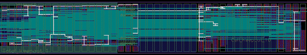
Figure 1. Routing result using standard ASIC style routing
Using ASIC-style tools to accelerate manual routing results in poor performance. These tools use a coarse global routing grid to divide the routing space, optimizing detailed routing within each global routing cell, but create discontinuities across the cells. This manifests itself as a serpentine routing of the ‘spine’ between pins, resulting in the use of additional wiring resource and more vias than is desirable. In datapath designs for example, this can lead to a 20% performance degradation relative to a spine routing scheme (Figure 1).
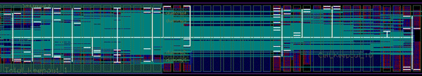
Figure 2. Equivalent routing using Spine and Stitch style
Unity incorporates special ‘spine and stitch routing’ to support optimum results and maximum performance for memory design. Coupled with specialized cluster placement, it delivers minimal bends and resulting net length. It also supports multiple areas and routing biases in designs that incorporate not only horizontal but also vertical device rows (Figure 2). Unity’s autoroute engine is ‘spine route’ aware, and its spine and stitch router obeys bus and shielding definitions; the main spines for defined buses are automatically generated adjacently, while buses (and normal nets) are shielded automatically.
Unity’s floorplanning and placement tools are also designed for the specific and unique requirements of custom design. The placement engine, interwoven with fast spine and stitch routing technology and working in unison with the floorplanning tool, is designed to handle a wide variety of components ranging from small cells or objects to blocks. This is in contrast to ASIC placers which only handle regular height standard cells.
ASIC tools, while allowing for grouping of cells, generally react poorly to fine-grained tight grouping of a large fraction of the design. For custom design, engineers need to be able to optimize the maximum performance from layout by ensuring the logical hierarchy is closely aligned to the final physical hierarchy, simulating logical sub-blocks with realistic physical data. This is known as clustering and cluster placement. Most ASIC floorplanners only support the planning of major functional blocks, and placing and routing takes place on a flat design. Unity gives designers full hierarchical block floorplanning.
Automatic and interactive block placement of soft and hard blocks incorporates reshaping of soft blocks as well as cut-outs in soft blocks to allow logic clusters. Automatic pin placement is possible and is able to handle rectilinear shapes and cut-outs. Full hierarchy manipulation is achieved by enabling designers to push and pop through blocks in the floorplan for implementation, and facilitating ‘edit-in-place’ functionality so block contents can be realized at higher levels. Designers also have the ability to ‘push down’ higher level routing into lower level blocks to achieve detailed implementation as the design becomes increasingly refined.
The flexible floorplanner (which generates regions and rows) drives automated placement. Rectilinear region and row support is available for non-rectangular block shapes from a higher-level block floorplan and includes support for cut-outs in block shape. Placement row generation can support a variety of models, including single rows with space separation, sets of rows (flipped and unflipped) with separation, and so forth. The placement engine supports custom digital cells of various sizes (including double height), is sensitive to SCM hierarchy and sub-circuits, and can recognize existing routing.
Unity has in-built homogeneous and hierarchical constraint management, which is consistent across floorplanning, placement and routing. All of the physical, electrical, object and inter-object relationships can be set as constraints. In addition, these can be applied in the front end (schematic) design environment, and passed through to the physical design. In this way, design intent can be set and held in the design environment then maintained throughout physical implementation. Design intent such as clustering, timing, width, spacing, length, shielding, matching, electrical resistance and capacitance (RC), and bias can be applied as constraints.
Design flow
A typical flow using Unity would be to define such constraints in the host-system schematics and to generate unplaced layout from them. After exporting into Unity, all the constraints would be applied. The block floorplan would be defined and global structures (such as power meshes or rails) pre-routed. Cells and devices obeying clusters can now be placed and the floorplan optimized, using compaction driven by spine estimation. After routing and balancing critical nets (including clocks), the majority of nets are ‘spined and stitched’. Automatic shape-based routing completes all nets, which are then tidied using built-in check-and-fix tools before exporting changes back into the host system, preserving new properties and floorplan details.
CDA solutions like Unity alleviate the pressure on design teams to deliver new and improved automated solutions in the highvolume IC arena. By providing an integrated and holistic approach, CDA overcomes the challenges inherent in complex, high-volume design scenarios, and delivers maximum profit.
Pulsic
150 Park Avenue
Aztec West
Bristol
BS32 4UB
UK
T : +44 (0)117 325 5000
W: www.pulsic.com