Addressing the design closure crisis
Why are more chips late to market and cost three times more to design at 90-nanometer (nm) than at 130nm? Today’s ASSPs and ASICs are huge, approaching one billion transistors, with clock speeds exceeding 1-GHz. Engineers struggle to manage the complexity of devices that achieve these levels of performance and size. A natural reaction to these challenges by semiconductor companies is to add more engineers to relieve the pressure, which drives up costs. And, yet the chips still takes twice as long to design, and the costs continue to increase. It is estimated that a 65nm ASSP will cost $55 million to develop.
Timing Closure Bottleneck
The most serious bottleneck in the IC design process is timing closure. Engineers use the timing closure flow throughout the design lifecycle to verify that the circuit design can be implemented. At the end of the design process, it is the last step before tape-out. In a typical design lifecycle, the implementation team will work with netlists for six months, experimenting with the implementation flow to feed back to the circuit design group modifications to meet the area, power, and timing specifications of the chip. They also continuously refine the recipe for implementing the chip that will be used to reach tapeout as quickly as possible in the final few weeks of the project.
Timing closure must be achieved in the routing step, which is where the wires that interconnect cells get created. Routers work with the placement and timing constraints to find resources for all of the wires while meeting specific process rules so that the chip will pass design rule checking (DRC). After routing, the chip is analyzed with a series of “sign-off” tools that have been certified by the process and library group of the target fab, as the final checkpoint to ensure the chip meets the design specification.
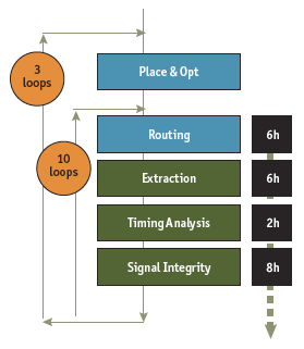
Figure 1. A typical timing closure flow
However, what was intended as a sign-off flow has actually become a timing optimization loop, which today is very time consuming and requires much manual intervention. In a typical attempt for timing closure, designers will make ten or more passes through the sign-off flow making cell substitutions, and implementing perturbations to placement in an attempt to reach closure. Typically, there are also at least three loops all the way back to circuit design that impact major areas of the chip. Each of these loops fixes a few problems and more often than not also creates a few more problems. This is a tedious task that goes on for weeks and months as the team works through hundreds, sometimes thousands, of timing and signal integrity violations.
Each pass through the sign-off loop typically takes more than one day, because the execution times of the tools are so long. Engineers painfully wait hours for extraction runs to complete so that they can then analyze and explore changes. Due to development schedule pressures, engineers end up attempting many changes simultaneously, which often perturbs more parts of the chip and causes even more new violations. The “analyze-correct” cycle begins all over again, with engineers waiting for the results from batch executions to find out if their changes are effective. Precious engineering resources are wasted rather than leveraged on value-add, creative design tasks.
Quality of Results Reduces Loops
To break the design closure bottleneck, a highly automated optimization platform is needed to collapse the sign-off loop — one that ensures high quality of results extremely fast with the capacity to handle the increasingly complex, larger chip designs of today and the future looking ahead to 65nm and beyond. Engineers need an “optimization system” that can automatically evaluate timing slacks, implement changes using design aware optimization routines, and then immediately analyze their impact, so that timing converges with minimal power and area cost. This requires the convergence of extraction, delay calculation, and timing analysis to deliver results that correlate to the accuracy of traditional signoff tools. Multi-variable optimization algorithms working concurrently with analysis provides the most effective and efficient method for achieving timing closure solutions with minimal impact to area or power consumption. The system must also simultaneously optimize for leakage power, signal integrity, electro-migration, and yield factors such as process variation.
The system must be incremental so that many areas of the chip are optimized simultaneously, enabling specific areas to be modified, analyzed, repaired, and reoptimized efficiently. As such, changes introduced independent of the sign-off process, such as late engineering change orders (ECOs), can be handled in a manner that maintains as much of the overall implementation as practical. This requires tiling and partitioning in the system which is tailored to the implementation or analysis task to be executed.
As the industry moves to smaller process geometries, the timing optimization problem becomes exacerbated by process variation. The optimization system must be architected to model timing in ways that takes into account the statistical and deterministic process variations that arise at 65nm and below. This includes both variations in wire width, as well as variations in wire thickness brought on by proximity effects and other lithography induced variations. In addition, the modeling of process corners will grow geometrically, which must be accommodated by parasitic extraction and timing analysis engines.
Extreme Speed through Multi-processing
The next-generation optimization system must also run at extreme speed so that the engineers can spend their time analyzing the output and exploring options, versus waiting for long runs to complete. Indeed, this is now a practical reality given the trend toward distributed, multi-processing utilizing relatively inexpensive farms of Linux computers. A multitude of factors must be carefully built into the underlying computing infrastructure of the optimization system, such as heterogeneous networks, total cost of ownership, multiple users, and how best to architect the software application for distributed multi-processing.
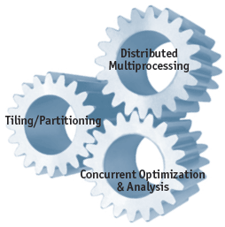
Figure 2. Driving more efficient closure
For example, the architecture of the EDA system must ensure that remote jobs are small enough so they can execute very quickly on machines with minimal memory configuration. This drives down the cost of the machines in the farm, and also facilitates more efficiently multiplexing of machines on different jobs for multiple users. Of course, the extreme speed must be enabled without increasing the complexity of managing the tools needed to run in the farm. Ideally, users should be given a simple way to specify only the computing and EDA license resources used during execution.
The system also must be architected such that when jobs are spawned into a farm, they run independently of each other to eliminate the need for messaging between machines. Multi-processing architectures that require data sharing in the network file system create a bottleneck that slows execution and makes debugging extremely difficult due to the dynamic nature of the network. With co-dependent jobs across multiple machines, an entire run is lost when just a single machine crashes. By contrast, remote execution of independent jobs utilizes a main machine to manage the creation, monitor the execution, and collect the output of the remote jobs across all machines.
For an EDA application such as optimization, this requires algorithms that tile the design in ways that are tailored to each task that will be executed. The tiling and partitioning algorithms must also take into consideration how the interdependencies between tiles will be managed, so that remote jobs can run independently.
Routing Optimization
With the proposed concurrent optimization and analysis platform, it is also important to consider global timing issues. To date, this has been the domain of placement optimization systems using estimates of the wires.
Fundamentally, IC routers provide solutions for the geometric problem of efficiently utilizing routing resources to properly wire all of the components on a chip. They also manage the process rules required to ensure DRC correct designs are implemented. Routers are very good at accomplishing both tasks. The most effective optimization for design closure uses the actual wires. However, it is not necessary to recreate the router to effectively optimize the routing process.
By leveraging the design tiling techniques described earlier, a “router independent” optimization system can seamlessly invoke third-party routers to perform detailed routing tasks. In this way, the routers are deployed to do what they do best, while also working in concert with the optimization system to converge the design to closure.
Summary
Engineers are struggling with timing closure because the sign-off flow has now become a manual optimization loop. The long run times of the tools in the flow make it increasingly difficult for them to complete even three loops in any given week. Because of this combination of manual processes and longer execution cycles chips are taking longer to implement. The net result is that companies miss their market windows, and the costs of design skyrockets as companies add more engineers to meet this challenge.
Athena Design Systems is a new EDA company with the mission, strategy and technologies to address the costly, acutely painful physical implementation challenges of complex, nanometer chip designs. The company will introduce a new class of IC optimization products that accelerate the productivity of engineers, design tools and compute resources enabling chip companies to reach design closure faster with higher quality of results and lower development costs.
Athena Design Systems
2900 Gordon Avenue
Suite 203
Santa Clara
CA 95051
USA
T: 1 408 522 1300
www.athenads.com