Chemical mechanical polish: the enabling technology
Chemical mechanical polishing (CMP) has traditionally been considered an enabling technology. It was first used in the early 1990s for BEOL metallization to replanarize the wafer substrate thus enabling advanced lithography, which was becoming ever more sensitive to wafer surface topography. Subsequent uses of CMP included density scaling via shallow trench isolation and interconnect formation via copper CMP.
As silicon devices scale to 45nm and beyond, many new uses of CMP are becoming attractive options to enable new transistor technologies. These new uses will demand improved CMP performance (uniformity, topography, low defects) at lower cost, and this will in turn require breakthroughs in hardware, software, metrology and materials (e.g., slurry, pad, cleaning chemicals).
This paper reviews the module level and integration challenges of applying traditional CMP steps to enable high-K metal gate for 45nm technology and to advance copper metallization from the 65nm to the 45nm node. These challenges are then considered with respect to new CMP applications for 32nm and beyond.
When Chemical Mechanical Polish (CMP) was first introduced to IC manufacturing in the early 1990s, common sense insisted that the process was too crude and riddled with defects to use in the production of modern electron devices. However, CMP overcame predictions of an early demise, and as the decade passed, its use expanded considerably. Table 1 shows the insertion of new CMP steps into logic IC technology nodes by year of insertion as well as the technology element enabled by each CMP step. Introduction of these early CMP steps was key to the IC manufacturers’ ability to maintain scaling trends.
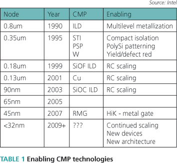
The insertion of new steps slowed during the first part of the current decade after the insertion of copper CMP at the 130nm node. A major reason for the slowdown was concern raised over CMP’s inadequacies—mainly that the technique was expensive, induced yield-limiting defect modes, and resulted in thickness variations that were inconsistent with the scaling trends of the IC industry. While the first implementations of CMP were required to enable technology scaling, the original concerns around its crudeness appeared to reassert themselves. During these years, methods were found to scale dimensions and improve transistor performance without requiring new CMP steps.
However, at the 45nm node, CMP is once again being used to enable a critical advancement in silicon technology. It is an integral component of the replacement metal gate (RMG) approach for defining metal gate structures required for high-k, metal gate (HKMG) dielectrics [1, 2]. Copper CMP has also been carried forward from the 65nm node to form Cu interconnects.
Requirements for RMG CMP
CMP technology is extensively utilized to create metal gate electrodes for the introduction of HKMGs at the 45nm technology node [1, 2]. Figure 1 shows the RMG process flow utilizing poly opening polish (POP) and metal gate polish steps. Because of the small dimensions and consequent small dimensional tolerance of the gate structure, traditional CMP processes are inadequate for these RMG steps. For functional devices and requisite yield, thickness control and defect performance has to be significantly improved over CMP processes used for previous technologies.
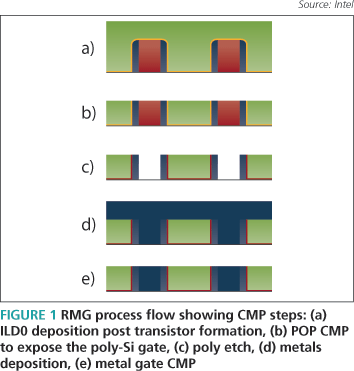
Table 2 shows integration issues associated with the insertion of the new RMG CMP steps. Many of these arise from insufficient thickness control, either during CMP or incoming to CMP. Low polish rates at the POP step result in tall gates that may not be properly filled with gate metals (due to high aspect ratio). Taller gates also require longer contact etch potentially resulting in underetched contacts. Severe underpolish, such that the poly-Si is not exposed, causes poly to remain in the gate, preventing proper metal fill. The resultant poly-Si gate transistor will fail due to improper work function (Vt shift) and high gate resistance.
Underpolishing at the metal CMP step results in incomplete overburden metal removal and hence shorting. The metal gate polish step must undergo sufficient overpolishing to remove any topography evolved during poly opening. Excessive overpolishing at either of the RMG CMP steps results in thin gates with high gate resistance and the potential for over-etched contacts. Severe overpolishing results in the exposure of the adjacent raised source/drain regions, which are then attacked in the post-CMP poly removal etch step. These integration concerns mean there is a narrow process window at both CMP steps.
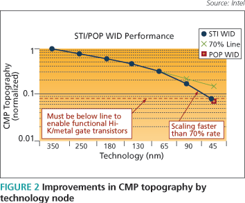
Figure 2 shows the historical improvements of within die (WID) thickness variation obtained for shallow trench isolation (STI)/POP CMP processes. Due to thickness control issues listed in Table 2, circuit yield declines precipitously for WID values above the dashed line. Note that historic 70% scaling from previous technologies is inadequate to meet required WID control.
The required thickness control is gained via several key CMP innovations. First WID/topography control is achieved by the selection of high selectivity slurry (HSS) and polish pad as well as the optimization of machine parameters around the selected set of consumables. With the HSS, the polish process slows significantly when the void-free interlayer dielectric (ILD0) overburden is cleared and the gate is exposed resulting in an autostop to the process. Next, within wafer (WIW) uniformity is optimized by structured experimental designs varying polish pressure, head and pad velocities, pad dressing and polish head design.
Thickness control within a standard edge exclusion is insufficient: poor polish control of the bevel region of the wafer potentially leads to subsequent redistribution of bevel films during poly etch and subsequent wet etch operations.
Significant CMP defect improvement is also required for satisfactory HMKG yield. Typical CMP defects are listed in Table 3 (these modes were experienced during the development of RMG CMP processes). Because of the narrow dimensions at the gate layer, HKMG yields are particularly sensitive to CMP defects, and without significant improvements from the initial levels of RMG CMP defects, HKMG yield would not have been viable.
Back-end metallization requirements
The scaling of circuit dimensions at the 45nm node also requires significant improvement to the copper CMP process. As the metal line width scales, variation in the height of the line results in greater variation in its resistance and capacitance. Copper metal loss during CMP (dishing and erosion effects) is a primary cause of interconnect height variation for the 45nm node, and a significant reduction in copper loss is required to ensure proper functioning of the interconnect.
Copper thickness loss is decreased as WIW and WID thickness control is raised, and also as improvements in surface topography at a given layer allow a reduction in the amount of oxide removed at subsequent layers. Underlying surface topography requires additional oxide removal to ensure that all of the metal overburden is removed from the low lying areas of the surface topography. Hence improvements in front-end topography translate into a need for less oxide removal in the upper back-end metal layers.
Improvements in the uniformity of the copper CMP WIW and WID removal rate at the 45nm node are a result of improvements in slurry selectivity as well as polish pad, pad dressing and polish machine parameter optimizations.
As with the RMG CMP steps, the defect modes listed in Table 3 are a challenge at copper CMP steps. Because modern IC technologies contain up to 10 layers of metal, even low levels of defect densities in the copper CMP step can have a significant impact on yield.
New uses of CMP
Recent conference proceedings and journal articles are rich with new potential uses of CMP, under consideration for 32nm and beyond. Table 4 lists some of those intriguing possibilities as well as some of the potential challenges they can be expected to bring. It is evident from all that activity that CMP is still considered useful by process technology architects.
However, the difficulties experienced in introducing RMG steps at the 45nm node demonstrate that any new CMP steps introduced into the front end of the line will require exceedingly tight film thickness and defect control. Without such control, recently added RMG CMP steps would not have successfully advanced from R&D to high volume manufacturing. Emerging options can be expected to demand even greater control of thickness and defects—as will shrinking to dimensions of 32nm, 22nm and beyond. To continue the growth of CMP, the industry must find processing conditions (slurry, pad, tooling) that improve performance in critical areas.
Acknowledgements
The author thanks Francis Tambwe, Matthew Prince and Gary Ding for assistance in preparing data, and Tahir Ghani and Anand Murthy for valuable discussions in preparing the manuscript.
References
- K.Mistry et al., IEDM Tech. Dig., p.247, (2007).
- C.Auth et al., Symp. VLSI Dig., p.128, (2008)
- K.Kuhn IEDM Tech. Dig., p.471, (2007).
- H.Y. Yu et al., IEDM Tech Dig., p.638, (2005).
- C. Park et al., IEDM Tech Dig., P.299, (2004).
- A. Kaneko et al., IEDM Tech Dig., p.884, (2005).
- Y-S Kim et al., IEDM Tech Dig., p.315, (2005).
- K.N. Chen et al., IEDM Tech Dig., (2006).
- S.M. Jung et al., IEDM Tech Dig., (2006).
- E.K. Lai et al., IEDM Tech Dig., (2006).
- D.C. Yoo et al., IEDM Tech Dig., (2006).
- T. Nirschl et al., IEDM Tech Dig., p.461, (2007).
Intel
RA3-301
2501 NW 229th Ave
Hillsboro
OR 97124
USA
T: 1 503 613-8472
W: www.intel.com
