Which ADC architecture is right for your application – Part Two
Selecting the proper ADC can appear a formidable task. A direct approach is to go to the selection guides and parametric search engines. Enter the sampling rate, resolution, power supply voltage, and other properties. Click ‘find’. But can one approach the task with greater understanding — particularly of the main architectures — and get better results? Most ADC applications can be classified into four broad market segments:
- data acquisition
- precision industrial measurement
- voiceband and audio
- ‘high speed’ (implying sampling greater than 5MSPS)
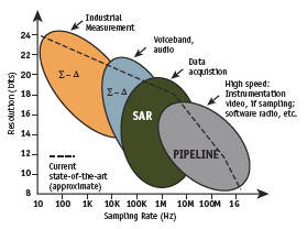 Figure 1. ADC architectures, applications, resolution, and sampling rates
A very large percentage can be filled by successive-approximation (SAR), sigma-delta (∑-Δ), and pipelined ADCs. Figure 1 shows in a general way how these application segments and the associated typical architectures relate to ADC resolution (vertical axis) and sampling rate (horizontal axis). The dashed lines represent the state-of-the-art in mid-2005. Even though the various architectures overlap, applications are key to making the right choice.
Here we shall concentrate on sigma-delta ADCs for voiceband and audio, and pipelined ADCs in ‘high speed’ applications. The first part of this article looked at SAR ADCs for data acquistion, and sigma-delta ADCs for precision measurement and instrumentation, and appeared in the December 2005 EDA Tech Forum. This is available for download from www.edatechforum.com or by selecting Analog Dialogue 39-06 online at the Analog Devices website (www.analog.com).
Sigma-Delta ADCs for voiceband and audio
In addition to providing attractive solutions for industrial measurement (precision measurement, sensor monitoring, energy metering, and motor control), the ∑-Δ converter dominates modern voiceband and audio applications. A major benefit of their high oversampling rate is that they simplify the input anti-aliasing filter for the ADC and the output anti-imaging filter for the DAC. In addition, the ease of adding digital functions to a CMOS-based converter makes features such as digital-filter programmability practical with only small increases in die area, power, and cost.
Digital techniques for voiceband audio began in the early days of PCM telecommunications applications in the 1940s. The early Tcarrier systems used 8-bit companding ADCs and expanding DACs, and a sampling frequency of 8 kSPS became the early standard. Modern digital cellular systems utilize higher-resolution oversampled linear ∑-Δ ADCs and DACs rather than the lower-resolution companding technique. Typical SNR requirements are 60dB to 70dB. If companding/expanding is required, it is done in the DSP hardware or software. Voiceband codecs have many applications other than PCM, such as speech processing and encryption, and various types are available.
∑-Δ ADCs and DACs also dominate the more demanding audio markets, including, FM stereo, stereo compact disc (CD), and DVD audio. Total harmonic distortion plus noise (THD + N) requirements range from 60dB to greater than 100dB, and sampling rates range from 48kSPS to 192kSPS. Modern CMOS ∑-Δ ADCs and DACs are up to these requirements and other digital functions associated with such applications.
Pipelined ADCs for high-speed applications (sampling rates greater than 5 MSPS)
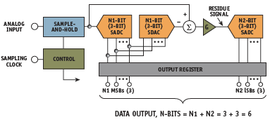 Figure 11. 6-bit, two-stage subranging ADC
In this article, we arbitrarily define any application requiring a sampling rate of greater than 5MSPS as ‘high speed’. Figure 1 shows that there is an area of overlap between SAR and pipelined ADCs for sampling rates between approximately 1MSPS and 5MSPS. Except for this small region, the applications considered high speed are most often served by a pipelined ADC. Today, the low-power CMOS pipelined converter is the ADC of choice, not only for video but for many other markets. Although lowresolution flash converters remain an important building block for the pipelined ADC, they are rarely used by themselves, except at extremely high sampling rates — generally greater than 1GHz or 2GHz — requiring resolutions no greater than 6 to 8 bits. Today, markets that require ‘high speed’ ADCs include many types of instrumentation applications (digital oscilloscopes, spectrum analyzers, and medical imaging). Also requiring high-speed converters are video, radar, communications (IF sampling, software radio, base stations, set-top boxes, etc.), and consumer electronics (digital cameras, displays, DVD, and high-definition TV).
The pipelined ADC has its origins in the subranging architecture, first used in the 1950s. A block diagram of a simple 6-bit, twostage subranging ADC is shown in Figure 11.
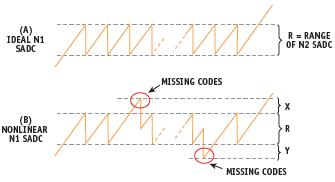 Figure 12. Residue waveform at input of secondstage SADC
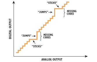
Figure 13. Missing codes due to MSB ADC nonlinearity or interstage misalignment
The output of the SHA is digitized by the first-stage 3-bit sub-ADC (SADC) — usually a flash converter. The coarse 3-bit MSB conversion is converted back to an analog signal using a 3-bit sub-DAC (SDAC). Then the SDAC output is subtracted from the SHA output, the difference is amplified, and this ‘residue signal’ is digitized by a second-stage 3-bit SADC to generate the three LSBs of the total 6-bit output word.
This subranging ADC can best be evaluated by examining the ‘residue’ waveform at the input to the second-stage ADC, as shown in Figure 12. This waveform is typical for a low-frequency ramp signal applied to the analog input of the ADC. For there to be no missing codes, the residue waveform must not exceed the input range of the second-stage ADC, as shown in the ideal case of Figure 12A. This implies that both the N1-bit SADC and the N1-bit SDAC must be accurate to better than N1 + N2 bits. In the example shown, N1 = 3, N2 = 3, and N1 + N2 = 6. The situation shown in Figure 12B will result in missing codes when the residue waveform goes outside the range of the N2 SADC, ‘R’, and falls within the ‘X’ or ‘Y’ regions — which might be caused by a nonlinear N1 SADC or a mismatch of interstage gain and/or offset. The ADC output under such conditions might appear as in Figure 13.
This architecture, as shown, is useful for resolutions up to about 8 bits (N1 = N2 = 4); however maintaining better than 8-bit alignment between the two stages (over temperature variations, in particular) can be difficult. It is worth noting that there is no requirement — other than certain design issues beyond the scope of this discussion — for an equal number of bits per stage in the subranging architecture. In addition, there can be more than two stages. Nevertheless, the architecture as shown in Figure 11 is limited to approximately 8-bit resolution unless error correction is added.
The error-corrected subranging ADC architecture appeared in the mid-1960s as a means to achieve higher resolutions, while still utilizing the basic subranging architecture. In the two-stage 6-bit subranging ADC, for example, an extra bit is added to the secondstage ADC which allows the digitization of the regions shown as ‘X’ and ‘Y’ in Figure 12. The extra range in the second-stage ADC allows the residue waveform to deviate from its ideal value — provided it does not exceed the range of the second-stage ADC. However, the internal SDAC must still be accurate to more than the overall resolution, N1 + N2.
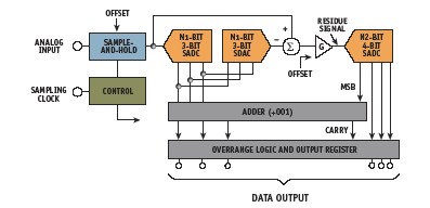 Figure 14. 6-bit subranging error-corrected ADC, N1 = 3, N2 = 4
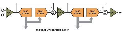
Figure 15. Generalized pipeline stages in a subranging ADC with error correction
A basic 6-bit subranging ADC with error correction is shown in Figure 14 (p28), with the second-stage resolution increased to 4 bits, rather than the original 3 bits. Additional logic, required to modify the results of the N1 SADC when the residue waveform falls in the ‘X’ or ‘Y’ overrange regions, is implemented with a simple adder in conjunction with a dc offset voltage added to the residue waveform. Here, the MSB of the second-stage SADC controls whether the MSBs are incremented by 001 or passed through unmodified.
It is worth noting that more than one correction bit can be used in the second-stage ADC, a trade-off — part of the converter design process — beyond the scope of this discussion. The error-corrected subranging ADC in Figure 14 does not have a pipeline delay. The input SHA remains in the hold mode during the time required for the following events to occur: the first-stage SADC makes its decision, its output is reconstructed by the firststage SDAC, the SDAC output is subtracted from the SHA output, amplified, and digitized by the second-stage SADC. After the digital data passes through the error correction logic and output registers, it is ready for use; and the converter is ready for another sampling-clock input.
To increase the speed of the basic subranging ADC, the ‘pipelined’ architecture (Figure 15) has become very popular. This has a digitally corrected subranging architecture in which each of the two stages operates on the data for one-half of the conversion cycle, and then passes its residue output to the next stage in the ‘pipeline’ prior to the next phase of the sampling clock. The interstage track-and-hold (T/H) serves as an analog delay line — it is timed to enter the hold mode when the first-stage conversion is complete. This allows more settling time for the internal SADCs, SDACs, and amplifiers, and allows the converter to operate at a much higher overall sampling rate.
Many trade-offs can be made in the design of a pipelined ADC, such as the number of stages, the number of bits per stage, number of correction bits, and the timing. To ensure the digital data from the individual stages corresponding to a particular sample arrives at the error correction logic simultaneously, the appropriate number of shift registers must be added to each of the outputs of the pipelined stages. So, if the first stage requires seven shiftregister delays, the next will require six, the next five, etc. This adds the digital pipeline delay to the final output data, as shown in Figure 16, the timing for a typical pipelined ADC, the AD9235. For the 12-bit, 65-MSPS AD9235, there are seven clock cycles of pipeline delay (sometimes referred to as latency). This latency may or may not be a problem, depending upon the application. If the ADC is within a feedback control loop, latency may be a problem — in the overlap area, the successive-approximation architecture would be a better choice. Latency also makes pipelined ADCs difficult to use in multiplexed applications. However, in most applications where frequency response is more important than settling time, latency is not a real issue.
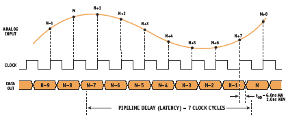 Figure 16. Timing of a typical pipelined ADC, the 12-bit, 65-MSPS AD9235
A subtle issue relating to most CMOS pipelined ADCs is their performance at low sampling rates. Because the internal timing generally is controlled by the external sampling clock, very low sampling rates extend the hold times for the internal trackand- holds to the point where excessive droop causes conversion errors. Therefore, most pipelined ADCs have a specification for minimum as well as maximum sampling rate. Obviously, this precludes operation in single-shot or burst-mode applications — where the SAR ADC architecture is more appropriate.
Finally, it is important to clarify the distinction between subranging and pipelined ADCs. Although pipelined ADCs are generally subranging (with error correction, of course), subranging ADCs are not necessarily pipelined. In fact, the pipelined subranging architecture is predominant because of the demands for high sampling rates, where internal settling time is of most importance.
Pipelined ADCs are available with resolutions of up to 14 bits and sampling rates over 100MHz. They are ideal for many applications that require high sampling rates and also a high signal-to-noise ratio (SNR) and spurious-free dynamic range (SFDR) (such as software-defined radios (SDR) for cellular base stations).
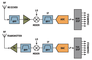 Figure 17. Generic IF-sampling wideband software radio receiver and transmitter
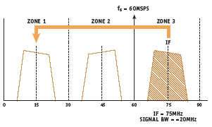
Figure 18. Sampling a 20-MHz BW signal with an IF frequency of 75 MHz at a sampling rate of 60 MSPS
Figure 17 shows a simplified diagram of a generic software radio receiver and transmitter. An essential feature is this: rather than digitize each channel separately in the receiver, the entire bandwidth containing many channels is digitized directly by the ADC. The total bandwidth can be as high as 20MHz, depending on the air standard. The channel-filtering, tuning, and separation are performed digitally in the receive-signal processor (RSP) by a high-performance digital signal processor (DSP).
Digitizing the frequency band at a relatively high intermediate frequency (IF) eliminates several stages of down-conversion. This leads to a lower-cost, more flexible solution in which most of the signal processing is performed digitally — rather than in the more complex analog circuitry associated with standard analog superheterodyne radio receivers. In addition, various air standards (GSM, CDMA, EDGE, etc.) can be processed by the same hardware simply by making appropriate changes in the software. Note that the transmitter in the software radio uses a transmit signal processor (TSP) and DSP to format the individual channels for transmission via the upstream DAC.
The ADC requirements for the receiver are determined by the particular air standards. The frequencies in the bandwidth presented to the ADC consist of the desired signals as well as largeamplitude ‘interferers’ or ‘blockers’. The ADC must not generate intermodulation products due to the blockers, because these unwanted products can mask smaller desired signals. The ratio of the largest expected blocker to the smallest expected signal basically determines the required SFDR. The ADC must have a SNR compatible with the required receiver sensitivity.
Another requirement is that the ADC meet the SFDR and SNR specifications at the desired IF frequency. The basic concept of IF sampling is shown in Figure 18, where a 20MHz band of signals is digitized at a rate of 60MSPS. Note how the IF sampling process shifts the signal from the third Nyquist zone to baseband without the need for analog down-conversion. The signal bandwidth of interest is centered in the third Nyquist zone at an IF frequency of 75MHz. The numbers chosen in this example are somewhat arbitrary, but they serve to illustrate the concept of undersampling. These applications place severe requirements on the ADC performance, especially with respect to SNR and SFDR.Modern pipelined ADCs can meet these demanding requirements. For instance, the AD9444 has an SFDR of 97dBc and an SNR of 73dB with a 70MHz IF input. The input bandwidth of the AD9444 is 650MHz.
Conclusion
This concludes our discussion of the successive approximation, ∑-Δ, and pipelined architectures.
Successive-approximation is the architecture of choice for nearly all multiplexed data acquisition systems, as well as many instrumentation applications.
For a wide variety of industrial measurement applications, the sigma-delta ADC is ideal; it is available in resolutions from 12 bits to 24 bits.
The ∑-Δ ADC and DAC, easily integrated into ICs containing a high degree of digital functionality, also dominate the voiceband and audio markets.
For sampling rates greater than approximately 5MSPS, the pipelined architecture dominates. These applications typically require resolutions up to 14 bits with high SFDR and SNR at sampling frequencies ranging from 5 to greater than 100MSPS. This class of ADCs is used in many types of instrumentation. Other applications are communications and consumer electronics. The use of manufacturers’ selection guides and parametric search engines, coupled with a fundamental knowledge of the three basic architectures, should help the designer select the proper ADC for the application. The use of manufacturers’ evaluation boards makes the process much easier. The Analog Devices’ ADIsimADC program allows the customer to evaluate the dynamic performance of the ADC without the need for any hardware. The software and the ADC models are free downloads at www.analog.com.
Not to be overlooked is the proper design of the ADC input, output, and sampling-clock circuitry. Data sheets and application notes should be consulted regarding these important issues. Finally, and equally critical are layout, grounding, and decoupling.
