What to look for when using an external PCB design center
The successful completion of complex PCB layouts requires a combination of highly skilled and experienced layout designers, a structured front-to-back design process, and advanced EDA toolsets. Success can be defined as meeting or exceeding all electrical, mechanical, and manufacturing requirements, and, where an external PCB design center is involved, satisfying the client in all interactions with them. This article considers each of those necessary components for success in turn and in greater detail.
The paper outlines the criteria upon which an OEM should make its selection of a third-party PCB design supplier. It groups these into three main categories.
- Staff with appropriate technical and communications skills.
- Comprehensive and fully documented design processes (ranging from the use of consistent design strategies to approaches to component library maintenance).
- Tool support to deliver appropriate time-to-market and manage increasing design (and design rule) complexity.
The successful completion of complex PCB layouts requires a combination of highly skilled and experienced layout designers, a structured front-to-back design process, and advanced EDA toolsets. Success can be defined as meeting or exceeding all electrical, mechanical, and manufacturing requirements, and, where an external PCB design center is involved, satisfying the client in all interactions with them. This article considers each of those necessary components for success in turn and in greater detail.
Designers
Competent people constitute the most important aspect of a successful PCB layout design, and they are absolutely critical when a project involves an external PCB design center. Most electronic or mechanical designs follow prescribed standards, but PCB projects require a degree of creativity that augments a designer’s ability to logically use layout tools and processes.
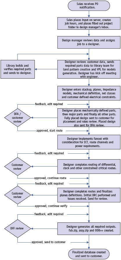
Figure 1. Layout flowchart
Designers must also have a good working knowledge of the predominant technologies in the market; communication skills so that they can interact intelligently with customer OEMs; and organizational skills so that they can keep track of the many facets of a complex design.
Most PCB design centers, including Optimum, do not require designers to be degree-level electrical engineers, although they must have a strong understanding of electrical concepts (e.g., high-speed, EMI Control, power distribution, etc).
When evaluating designers, it is important to determine whether candidates have kept abreast of technological trends and advances (e.g., attended courses, user group meetings, etc). They should also be flexible enough to take advantage of the wealth of knowledge that OEM clients bring to a project.
Designers should be able to recognize the special design considerations required for each circuit type (e.g., memory, processor, power supply, I/O interfaces and other industry standards). They must also understand the implications of industry-standard form factors (e.g., PCIe, VME, and ATCA), especially their mechanical and electrical constraints. To implement these common circuits and form factors, it is vital that the designer understands the various component application notes and related industry guidelines to ensure optimal performance. Some standards are relatively simple, but many are extremely complex, such as processor design guidelines and memory technologies (DDR1-3). With today’s fast clocking rates creating timing and EMI challenges, it is imperative that designers are also well versed in these potential roadblocks and intimately familiar with techniques that address them. Often clients are not familiar with all aspects of these complex specifications and therefore rely heavily on the expertise of PCB contractor’s designers.
Communication
Regardless of a designer’s technical prowess, his or her single most important skill must be an ability to communicate with the customer to ensure a timely flow of information. The designer must have enough technical savvy to know what technologies and background detail are required for a specific design, and, in that context, must then be confident enough to pursue further information without being apprehensive about asking any question, no matter how trivial it may seem.
It is also extremely important that the entire layout team (designer, engineers, and management) is ‘in sync’ regarding project expectations. This is best accomplished by having a ‘kick-off ’ meeting during which all technical and schedule goals are discussed and agreed. For any project, questions will arise and decisions need to be made during the layout. For example, engineers often overly constrain routing requirements to a point where the desired result will either take far too long to complete or even be unattainable. An external PCB design center should proactively contribute to the work that defines the project’s ideal constraints, so that the required specification is delivered at reasonable cost and on schedule.
The critical criterion for communication is to create an environment where nothing is assumed. To achieve this, Optimum places prime emphasis on the creation of a highly structured layout methodology. The use of scripts, checklists, and travelers ensures that all aspects of a design are taken into account fully. This structured layout flow creates an environment where all specifications are met and the design is kept on schedule.
Figure 1 (p.42) shows the comprehensive checklist used by the company today. It is the result of years of experience and has evolved through numerous iterations. It demonstrates the level of detail that we apply to every project and can be used as a benchmark when evaluating PCB design centers.
Process
If left unchecked, designers’ unconstrained creativity can lead them to create layouts that are completely different in every way, one from another. To avoid this, we have created a front-to-back, documented design process to ensure that every layout has the same look and feel and yet still allows each designer to exercise some necessary creative license. Every competent PCB design center should have a similar process, and the checklist in Figure 1 represents just one aspect of this larger strategy. A comprehensive companion designer’s handbook is also essential to producing creative designs that still meet well-defined standards and practices.
The flow is generally the same for all designs: mechanical definition, placement, planes and routing, silkscreen, and outputs. What differentiates the top rank of design centers is how they approach each of these phases from the viewpoint of signal integrity, manufacturability (fabrication, assembly, and test), and overall speed and efficiency. Optimum ensures that its layouts are consistent by having staff adhere to time-tested practices documented in its designer’s handbook; by utilizing a project checklist on every design; and through weekly meetings where current projects are discussed and the team is updated on the market’s ever-changing technologies.
Another critical part of the design process comprises comprehensive libraries of component datasheets, application notes, design practices, and materials technology. High quality and consistent library creation is the foundation of a successful layout process.
The typical design process begins with a project request and definition. When Optimum receives the bill of materials, it is passed along to our library group in the form of a request to identify or create any missing component footprints not already in our master library. Where a part is identified as new, it will be built to IPC7351 standards and then verified by one of the other librarians before being added. Errors in creating component footprints can have catastrophic consequences, so the best PCB design centers will demonstrate how they use checks and balances to keep layout libraries up-to-date and error-free.
Cornerstones
The following design example highlights key techniques and processes based on Optimum’s approach to signal integrity, manufacturability, and efficiency. Placement is typically the most critical phase, and designers must have sufficient time to ensure that the board can be routed and assembled in the most efficient manner.
Components are spaced to have proper clearances from each other; bypass capacitors are placed in close proximity to device pins per specification; termination circuits are placed appropriately at the source or load; and manufacturers’ application notes are reviewed and implemented for the best fit. Once the placement is complete and approved by the client’s engineering staff, an automated designfor- assembly (DFA) analysis must be run, verifying all component spacing and land patterns for correctness.
Component fan-out is also important. A well-constructed fan-out strategy has many benefits. Through proper via-to-via spacing rules, all nets can be successfully connected to the fewest number of layers and 100% coverage for in-circuit-test (ICT) is much easier to achieve. When databases do not enable sufficient care to be taken in the fan-out of high current signals, one result may be that large tantalum capacitors and voltage regulators have only one small via stitched to the plane layer. A sufficiently detailed infrastructure will ensure that larger vias are used and stitch in as many as reasonable to minimize inductance and maximize current capacity.
Layer stack-ups are also fundamental to an effective structured layout process. Our designer’s handbook dedicates many pages to strategies for layer symmetry, copper balancing, power and ground groupings, core thicknesses, crosstalk, and impedances.
Once the design is complete and all the items on the project checklist have been satisfied, the database is sent back to the client’s project engineer for approval. Upon approval, we put together a very comprehensive output package that consists of all the files needed for manufacturing. The last step in the design process is to run the outputs through automated design-for-fabrication (DFF) analysis software to ensure all outputs are correct and that nothing has been omitted.
Tools
Customers may specify a particular design software tool for PCB layout. When one is not specified, we prefer the Expedition series from Mentor Graphics for complex designs. Any EDA layout tools can be used to design a board, but when designing complex PCBs it is critically important to use the right tool for efficiency, rules integrity, and database reliability.
Most of today’s complex designs require a very large number of mechanical and signal constraints. Some rules are relatively basic, but many are so complex that tracking compliance by hand is virtually impossible. You must use layout tools that are ‘rules driven’ and that accept complex and vast rule sets. Once all the rules are built in the database, a designer can interactively place and route a layout according to his or her personal style. Tracking compliancy with all rules, through metrics, reports, and a postdesign rule check is essential to design validation.
Time-to-market is a major issue. Even with highly skilled and efficient designers, it would be difficult to complete many complex PCBs within today’s ultra competitive deadlines without proper tools. Having tools such as Mentor’s Xtreme PCB allows us to have multiple designers working on the same design simultaneously in a real-time environment. Concurrent design flows with high capacity interactive routing tools allow you to shave days, even weeks off cycle times.
Once the project is complete, designers can be confident in the integrity of the database and that the manufacturing outputs will match the original specifications.
Conclusion
Working with an external PCB design center can be a program savior or a stressful endeavor. Selecting the wrong house can result in issues far more insidious than just missing your market launch date. A poorly designed PCB can be wrought with EMI problems that can take considerable time to locate and remedy — if they can be fixed at all. Crosstalk and inductive coupling can cause problems that may not even show up until the product is in full production. In short, a great product can be killed by poor PCB design layout.
The three keys to selecting a competent, quality PCB design center are creative designers working within the constraints of comprehensive, documented processes and equipped with the state-of-art tools to ensure that the design layout meets the customer’s mechanical, electrical and schedule specifications.
Optimum Design Associates
1075 Serpentine Lane
Pleasanton
CA 94566
USA
T : +1 925 401 2004
W: www.optimumdesign.com
